Chip resistor

a chip resistor and resistor layer technology, applied in the direction of resistors, resistor details, adjustable resistors, etc., can solve the problems of difficult to obtain given resistance value, difficult to obtain low resistance value of chip resistor 10, etc., to achieve high accuracy, low resistance value, and increase the sectional area of the resistor layer

Inactive Publication Date: 2002-09-12
ROHM CO LTD
View PDF3 Cites 6 Cited by
  • Summary
  • Abstract
  • Description
  • Claims
  • Application Information

AI Technical Summary

Benefits of technology

0006] It is a first object of the invention to provide a chip resistor capable of obtaining a low resistance value compared with a conventional chip resistor, e.g. a resistance value of about 1 .OMEGA. to 1 K .OMEGA., and also capable of adjusting a resistance value by trimming a resistor layer with high accuracy compared with the conventional chip resistor by increasing a sectional area of the resistor layer.

Problems solved by technology

Further, since the entire size of the resistor layer 3 is very small to an extent of about 0.3.times.0.6 mm, it is convenient for the chip resistor 10 to obtain a high resistance value but it is not easy for the chip resistor 10 to obtain a low resistance value.
However, since the sectional area S1 is small, there is a limit to apply trimming to the resistor layer as a matter of course so as to adjust the resistance value, an hence since an adjustable range of the resistance value is small, a given resistance value is not easily obtained.

Method used


Image

  • Chip resistor
  • Chip resistor
  • Chip resistor

Examples


Embodiment Construction

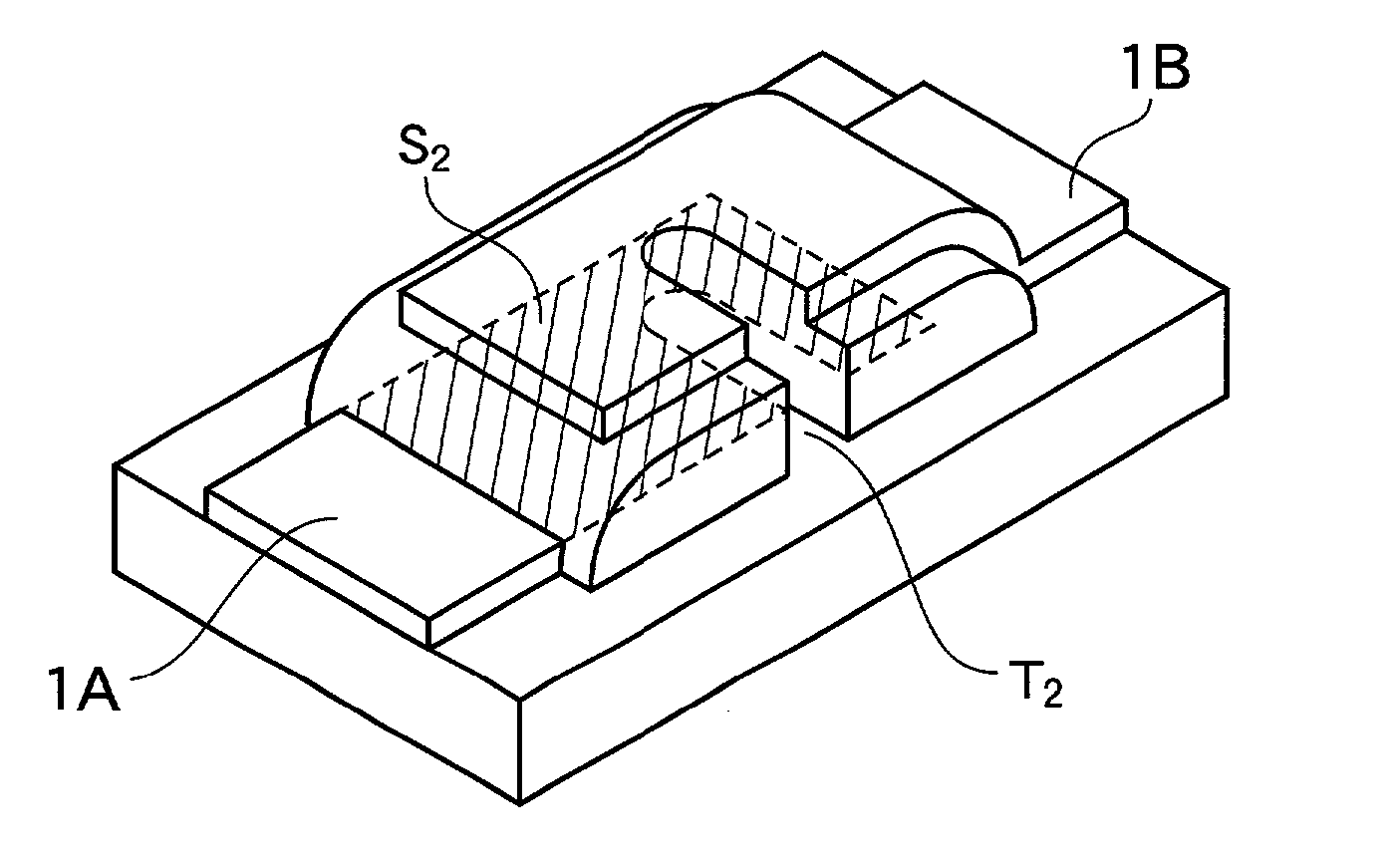
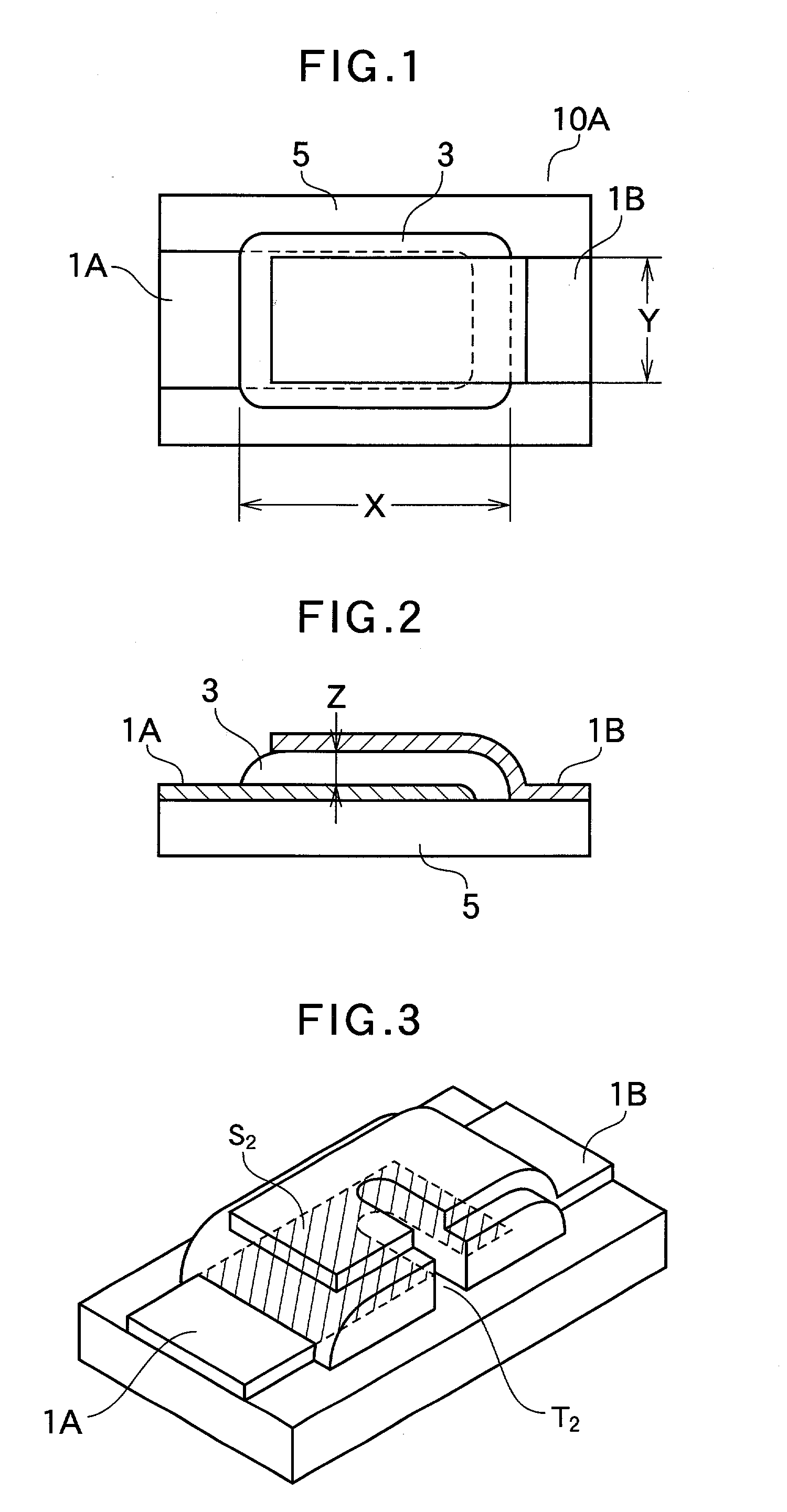
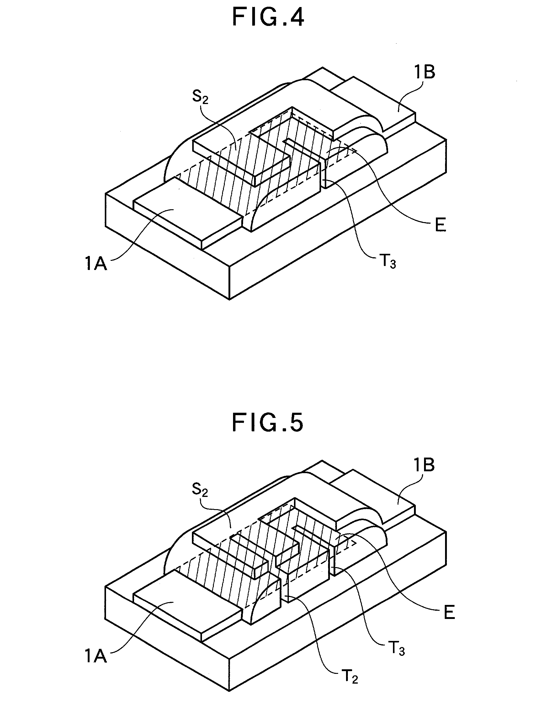
[0022] FIG. 1 is a view for explaining the construction of a chip resistor 10A according to a preferred embodiment of the invention.

[0023] The chip resistor 10A comprises a first electrode 1A made of gold or silver paste and formed on a substrate 5 made of, e.g. alumina in the same manner as the conventional chip resistor, a resistor layer 3 provided on the first electrode 1A, and a second electrode 1B provided on both the resistor layer 3 and substrate 5.

[0024] That is, the chip resistor 10A has a three-layered structure wherein the first electrode 1A and second electrode 1B are disposed on the substrate 5 while sandwiching the resistor layer 3 therebetween.

[0025] Since an effective sectional area S2 of the resistor layer 3 between the first electrode 1A and second electrode 1B of the chip resistor 10A taken along a line in parallel with the first electrode 1A and second electrode 1B has a laminated structure in which the first electrode 1A and the second electrode 1B shown in FIG....


PUM


Abstract

A chip resistor having a highly accurately adjusted low resistance value is obtained. The chip resistor having a vertically three-layered structure is obtained by forming a first electrode 1A by printing paste for an electrode on an insulating substrate 5 and drying it, a resistor layer 3 by printing paste for a resistor on the first electrode 1A and drying it, a second electrode 1B by printing paste for an electrode on the resistor layer 3 and the insulating substrate 5 and baking it. Trimming is applied to the thus fabricated chip resistor so as to adjust a resistance value to a given value.

Description

FIELD OF THE INVENTION[0001] The invention relates to a chip resistor having a low resistance, particularly to a chip resistor having a resistance value which is adjusted to a low resistance value.BACKGROUND OF THE INVENTION[0002] A chip resistor has been widely used for a resistor in view of high density, downsizing and the like of a circuit as an IT (information technology) associated equipment and the like have become recently widespread. A conventional chip resistor comprises, as illustrated in FIG. 6 showing a plan view and FIG. 7 showing a side view, a pair of first electrodes 1 formed by printing a conductive paste comprised of precious metals such as Au, Ag or Au--Pt or comprised of Cu, Al or Ni based material on an insulating substrate 5 (hereinafter referred to as simply substrate 5) made of a material such as alumina, steatite, forsterite and the like by screen printing and the like, and baking the printed conductive paste, and a resistor pattern formed by printing paste ...

Claims


Application Information

Patent Timeline
Patent Type & Authority Applications(United States)
IPC IPC(8): H01C7/00H01C17/24
CPCH01C7/003H01C17/24
Inventor TSUKADA, TORAYUKINONAKA, MITSUO
Owner ROHM CO LTD
Why Eureka
Try Eureka