Semiconductor device having trench isolation layer and a method of forming the same

a technology of isolation layer and semiconductor device, which is applied in the direction of semiconductor device, electrical apparatus, transistor, etc., can solve the problems of difficult to change the sog layer into a perfect oxide silicon layer, the method is not suitable for filling a trench having a very high aspect ratio, and the width of the trench in which the isolation layer is formed also decreases

Inactive Publication Date: 2002-09-12
SAMSUNG ELECTRONICS CO LTD
View PDF0 Cites 46 Cited by
  • Summary
  • Abstract
  • Description
  • Claims
  • Application Information

AI Technical Summary

Problems solved by technology

However, as integration density of the semiconductor memory device increases, the width of the trench in which the isolation layer is formed is also diminished.
However, such a method is not suitable for filling a trench having a very high aspect ratio, e.g., a width of about 1200 .ANG. and a depth of about 6000 .ANG..
But it is difficult for the SOG layer to change into a perfect oxide silicon layer, even though a recovery process for changing the SOG layer into an oxide silicon layer is performed through successive heat treatment.
A disadvantage of use of a SOG layer is ...

Method used


Image

  • Semiconductor device having trench isolation layer and a method of forming the same
  • Semiconductor device having trench isolation layer and a method of forming the same
  • Semiconductor device having trench isolation layer and a method of forming the same

Examples


Embodiment Construction

[0016] The present invention will now be described more fully hereinafter with reference to the accompanying drawings, in which preferred embodiments of the invention are shown. This invention may, however, be embodied in different forms and should not be construed as limited to the embodiments set forth herein. Rather, these embodiments are provided so that this disclosure will be thorough and complete, and will fully convey the scope of the invention to those skilled in the art. In the drawings, the thickness of layers and regions are exaggerated for clarity. It will also be understood that when a layer is referred to as being "on" another layer or substrate, it can be directly on the other layer or substrate, or intervention layers may also be present. Moreover, each embodiment described and illustrated herein includes its complementary conductivity type embodiment as well. Like numbers refer to like elements throughout.

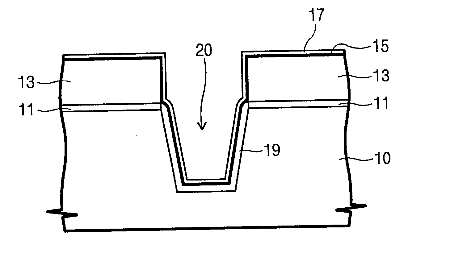
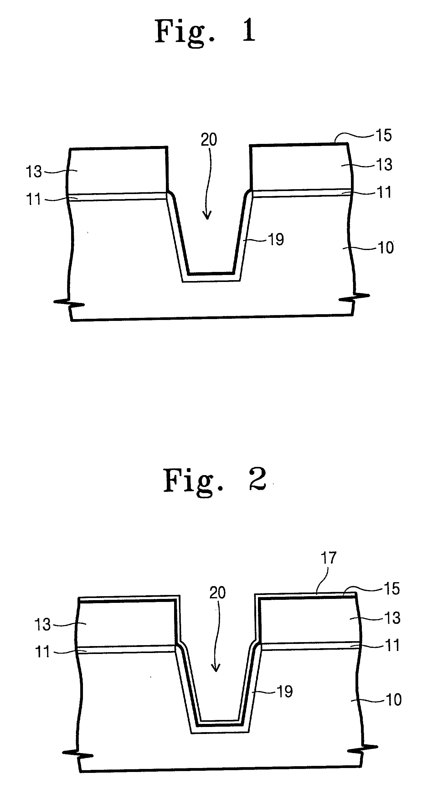
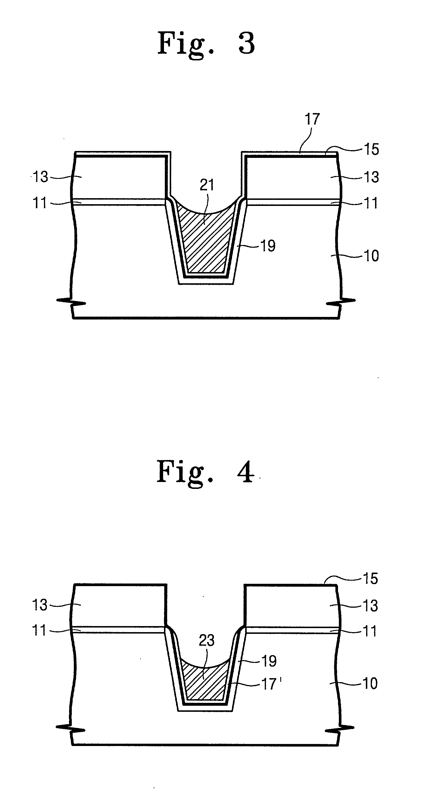
[0017] FIG. 1 illustrates the steps of forming a trench 20 o...


PUM


Abstract

A semiconductor device having a trench isolation layer in a semiconductor substrate is provided, wherein the trench isolation layer includes a silicon nitride liner, a silicon oxide liner; and a buried layer, wherein the buried layer includes a first buried layer for filling a lower part of the trench isolation layer and a second buried layer for filling an upper part of the trench isolation layer. A semiconductor device preferably further includes a silicon oxide layer disposed between the semiconductor substrate and the silicon nitride liner. The silicon oxide layer includes a thermal oxide layer densified at a temperature over about 800.degree. C.

Description

RELATED APPLICATION[0001] This application claims priority to Korean Patent Application No. 2001-12603, filed on Mar. 12, 2001, the contents of which are herein incorporated by reference in their entirety.FIELD OF THE INVENTION[0002] The present invention relates to a semiconductor device and a fabrication method therefor, and more particularly, to a semiconductor device having a trench isolation layer and a fabrication method therefor.BACKGROUND OF THE INVENTION[0003] As integration density of semiconductor memory devices (e.g., DRAMs) increases, circuit components such as transistors are formed closer to each other and reliability of the devices decreases unless effective isolation techniques for separating devices such as MOS transistors next to each other are employed. Trench isolation techniques which can form an isolation region having a narrow width are widely used in the manufacture of highly integrated semiconductor memory devices. Other conventional isolation methods inclu...

Claims


Application Information

Patent Timeline
IPC IPC(8): H01L21/76H01L21/762
CPCH01L21/76224Y10S438/978H01L21/76
Inventor HEO, JIN-HWAHONG, SOO-JIN
Owner SAMSUNG ELECTRONICS CO LTD
Why Eureka
Try Eureka