Thin film transistor array panel for a liquid crystal display and methods for manufacturing the same
Inactive Publication Date: 2002-09-19
SAMSUNG DISPLAY CO LTD
View PDF0 Cites 87 Cited by
Summary
Abstract
Description
Claims
Application Information
AI Technical Summary
This helps you quickly interpret patents by identifying the three key elements:
Problems solved by technology
Method used
Benefits of technology
Benefits of technology
0040] It is preferable that the lower conductor layer is made of indium tin oxide or transparent conductive materials and an ohmic contact layer pattern made of silicide or microcrystalized doped amorphous silicon to reduce the contact resistivity between th
Problems solved by technology
It may cause a disconnection of the pixel electrode near the high step-up area.
Han et al. has a problem of forming a wid
Method used
Image
Click on the blue label to locate the original text in one second.
Reading with bidirectional positioning of images and text.
Examples
Example
[0089] Now, a manufacturing method for a thin film transistor array panel according to the first embodiment of the present invention will be described with reference to FIGS. 6A to 8C as well as to FIGS. 3 to 5.
[0090] FIG. 6A is a layout view of a TFT array panel in the first manufacturing step according to the first embodiment of the present invention, FIGS. 6B and 6C are the cross-sectional views taken along the lines VIB-VIB' and VIC-VIC' of FIG. 6A, respectively. FIG. 7A is a layout view of a TFT array panel in a manufacturing step following FIGS. 6A to 6C. FIGS. 7B and 7C are the cross-sectional views taken along the lines VIIB-VIIB' and VIIC-VIIC' of FIG. 7A, respectively. FIG. 8A is a layout view of a TFT array panel in a manufacturing step following FIGS. 7A to 7C, and FIGS. 8B and 8C are the cross-sectional views taken along the lines VIIIB-VIIIB' and VIIIC-VIIIC' of FIG. 8A, respectively.
[0091] First, as shown in FIGS. 6A to 6C, a transverse gate wire including a plurality...
Example
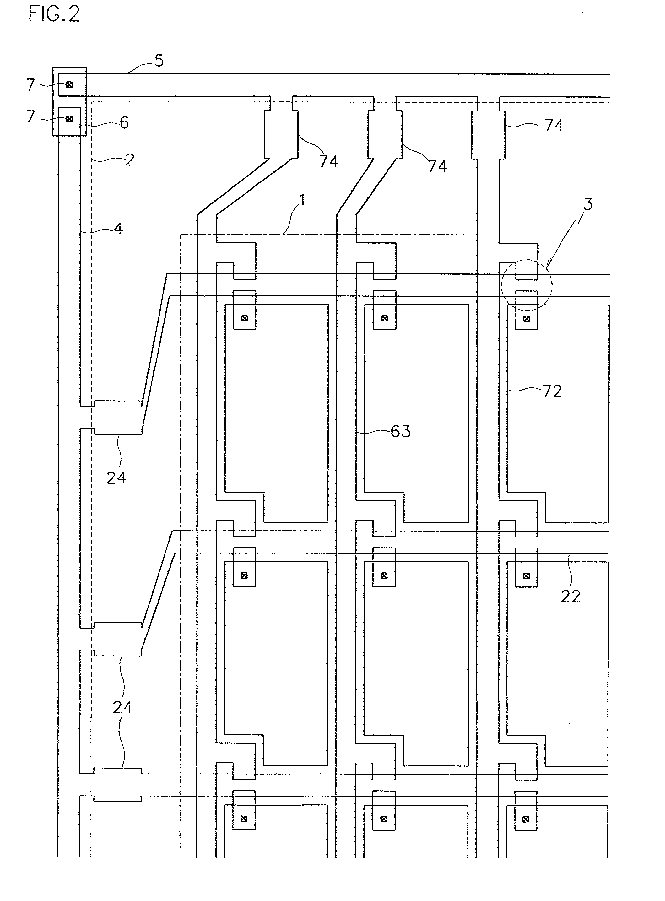
[0099] FIG. 9 is a layout view of a TFT array panel for an LCD according to the second embodiment of the present invention.
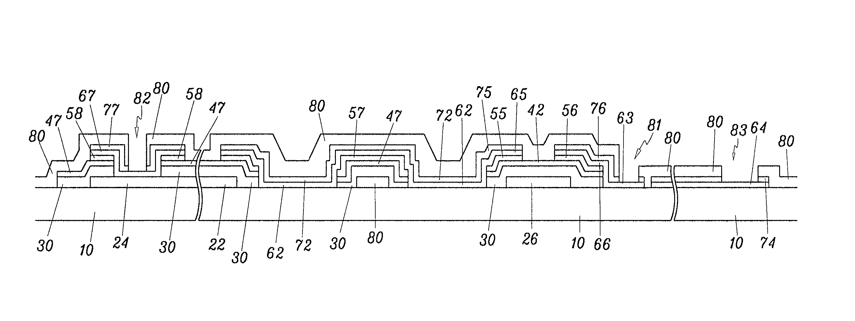
[0100] As shown in FIG. 9, a pixel electrode 63 has on opening 68 with a shape of slit pattern to widen viewing angle. The curved fringe field formed at the edges of the opening 68 forms multi-domains where the average direction of the molecular axes of the liquid crystal layer are different from those in one pixel region, thereby enlarging viewing angle. The number of the openings in a pixel may be larger than one.
[0101] According to the present invention, the TFT array panel for the liquid crystal display can be manufactured by using the four photolithography steps, and the gate pads are sufficiently protected. In addition, the leakage current of the liquid crystal display is effectively reduced.
[0102] Next, photomasks having different transmittance depending on position in the step of patterning the gate insulating layer, the semiconductor layer and the ohmic...
Example
[0104] FIG. 10 is a layout view of a TFT array panel for an LCD according to the third embodiment of the present invention, and FIGS. 11 and 12 are cross-sectional views respectively taken along the line XI-XI and XII-XII' of the FIG. 10.
[0105] A gate wire of metal or conductive material such as aluminum (Al) or aluminum alloy, molybdenum (Mo) or molybdenum-tungsten (MoW) alloy, chromium (Cr) and tantalum (Ta) is formed on an insulating substrate 10. The gate wire includes a plurality of gate lines (scanning signal lines) 22 extending in the horizontal direction, a plurality of gate pads 24 which are connected to one ends of the respective gate line 22 and a transmit a scanning signals from an external circuit to the gate line 22, a plurality of gate electrodes 26 of TFTs, which are branches of the gate lines 22.
[0106] The gate wire 22, 24 and 26 may have a multiple-layered structure as well as a single-layered structure. When the gate wire 22, 24 and 26 has the multiple-layered str...
PUM
Abstract
A gate wire is formed on an insulating substrate by a photolithography process using the first mask, and a gate insulating layer and a semiconductor layer are sequentially deposited. Then, an ohmic contact layer made of silicide or microcrystallized and doped amorphous silicon is formed on the semiconductor layer. Then, a triple pattern including a gate insulating layer, a semiconductor layer and an ohmic contact layer are patterned at the same time by a photolithography process using the second mask. At this time, a contact hole exposing the gate pad is formed. An ITO layer and a metal layer are deposited and patterned to form a data wire, a pixel electrode, and a redundant gate pad by a photolithography process using the third mask. The ohmic contact layer, which is not covered with the ITO layer and the metal layer, is removed. A passivation layer is deposited and patterned by a photolithography process using the fourth mask. Next, the metal layer of the pixel electrode, the redundant gate pad, and the data pad, which is not covered with the passivation layer, is removed. At this time, the semiconductor layer that is not covered with the passivation layer is removed to separate the semiconductor layer under the neighboring the data lines.
Description
BACKGROUND OF THE INVENTION[0001] (a) Field of the Invention[0002] The present invention relates to a thin film transistor (TFT) panel for a liquid crystal display (LCD) and methods for manufacturing the same.[0003] (b) Description of the Related Art[0004] An LCD is one of the most popular flat panel displays (FPDs). The LCD has two panels having two kinds of electrodes that generate electric fields and a liquid crystal layer interposed therebetween. The transmittance of incident light is controlled by the intensity of the electric field applied to the liquid crystal layer.[0005] The field-generating electrodes may be formed at each of the panels or at one of the panels. One of the panels having at least one kind of the electrodes has switching elements such as thin film transistors.[0006] In general, a TFT array panel of an LCD includes a plurality of pixel electrodes and TFTs controlling the signals supplied to the pixel electrodes. The TFT array panel is manufactured by photolith...
Claims
Application Information
Patent Timeline
Application Date:The date an application was filed.
Publication Date:The date a patent or application was officially published.
First Publication Date:The earliest publication date of a patent with the same application number.
Issue Date:Publication date of the patent grant document.
PCT Entry Date:The Entry date of PCT National Phase.
Estimated Expiry Date:The statutory expiry date of a patent right according to the Patent Law, and it is the longest term of protection that the patent right can achieve without the termination of the patent right due to other reasons(Term extension factor has been taken into account ).
Invalid Date:Actual expiry date is based on effective date or publication date of legal transaction data of invalid patent.

