Manufacturing Method Of Semiconductor Device

Active Publication Date: 2015-08-13
TOYODA GOSEI CO LTD
View PDF9 Cites 1 Cited by
  • Summary
  • Abstract
  • Description
  • Claims
  • Application Information

AI Technical Summary

Benefits of technology

The patent is about a new invention that reduces the contact resistivity between a semiconductor substrate and a metal layer. The invention includes several components that can be changed, omitted, or replaced with other components to achieve certain technical effects. The invention can be implemented in various aspects such as the manufacturing method of the semiconductor device or power conversion equipment. Overall, the invention improves the performance and reliability of semiconductor devices and power conversion equipment.

Problems solved by technology

The technique described in JP 2007-508093 is thus not sufficient as the method of reducing the contact resistivity.
This known technique needs the process of removing the silicon dioxide film after deposition of the silicon dioxide film on the N surface and accordingly has the problem of increased manufacturing cost.
The manufacturing method of the semiconductor device of this aspect reduces the contact resistance between the semiconductor substrate and the metal layer.
The manufacturing method of the semiconductor device of this aspect further reduces the contact resistance between the semiconductor substrate and the metal layer.

Method used


Image

  • Manufacturing Method Of Semiconductor Device
  • Manufacturing Method Of Semiconductor Device
  • Manufacturing Method Of Semiconductor Device

Examples


first embodiment

A. First Embodiment

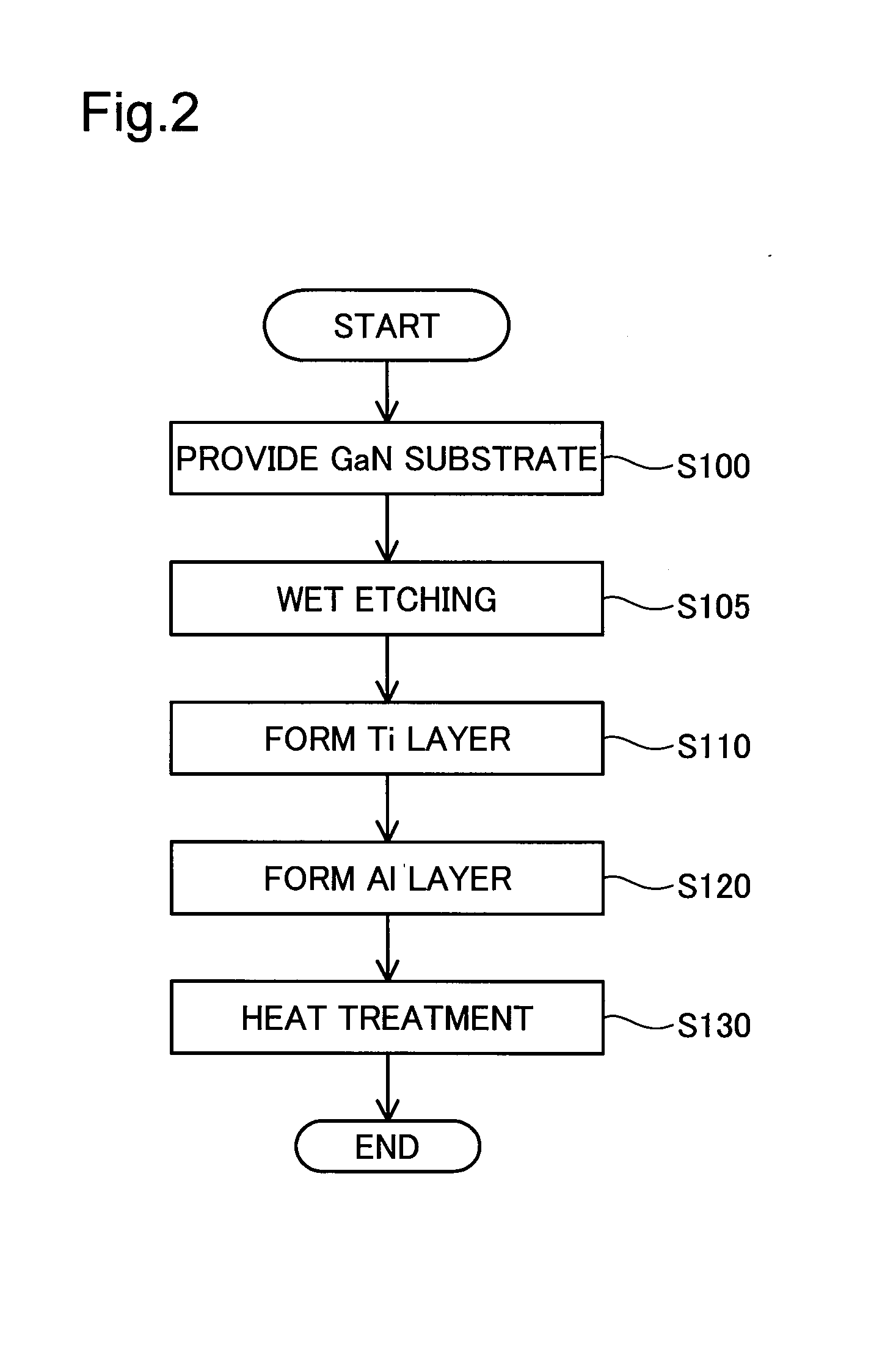
[0025]A1. Structure of Semiconductor Device 100

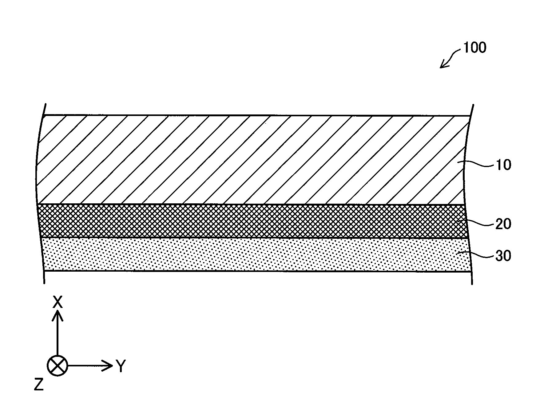
[0026]FIG. 1 is a cross sectional view schematically illustrating the structure of a semiconductor device 100 according to a first embodiment. FIG. 1 illustrates part of the cross section of the semiconductor device 100 according to the embodiment. FIG. 1 is a diagram for the purpose of illustrating the technical feature of the semiconductor device 100 in an easily understandable manner and does not represent the thicknesses of the respective layers correctly. XYZ axes orthogonal to one another are also shown in FIG. 1, in order to facilitate the explanation. In the description herein, thickness of a layer means thickness in an X-axis direction.

[0027]The semiconductor device 100 of this embodiment is SBD (Schottky Barrier Diode). The semiconductor device 100 includes a semiconductor layer 10, a titanium layer 20 and an aluminum layer 30.

[0028]The semiconductor layer 10 is mainly made of a nitride semiconductor. Availa...

modification 5

C5. Modification 5

[0063]In the above embodiment, the semiconductor device is SBD. The invention is, however, not limited to this structure. The semiconductor device may be FET (field effect transistor), bipolar transistor, IGBT (insulated gate bipolar transistor) or PIN (p-intrinsic-n) diode.

[0064]C6. Modification 6

[0065]In the above embodiment, the method forms the metal layer by sputtering at the film formation rate controlled to 4 nm / minute or lower. The invention is, however, not limited to this procedure. A modified procedure may form a metal layer by sputtering at the film formation rate controlled to be higher than 4 nm / minute after the process of forming the metal layer by sputtering at the film formation rate controlled to 4 nm / minute or lower (first process). The process of forming the metal layer by sputtering at the film formation rate controlled to be higher than 4 nm / minute is called second process. Controlling the film formation rate to be higher than 4 nm / minute in t...


PUM


Abstract

A technique of reducing the contact resistance between a semiconductor substrate and a metal layer is provided. A manufacturing method of a semiconductor device comprises a process of forming a metal layer on an N surface of a nitride semiconductor substrate. The process of forming the metal layer includes a first process of forming a metal layer by sputtering at a film formation rate controlled to 4 nm / minute or lower.

Description

CROSS-REFERENCE TO RELATED APPLICATION[0001]The present application claims priority from Japanese patent applications No. 2014-24228 filed on Feb. 12, 2014, the entirety of disclosures of which is hereby incorporated by reference into this application.FIELD OF INVENTION[0002]The invention relates to a manufacturing method of a semiconductor device.DESCRIPTION OF RELATED ART[0003]A known method of reducing the contact resistivity between an N surface of a nitride semiconductor substrate such as gallium nitride (GaN) substrate and an electrode makes a silicon dioxide (SiO2) film deposit on the N surface, removes the silicon dioxide film and subsequently forms an electrode (JP 2007-508093).SUMMARY[0004]The technique described in JP 2007-508093, however, the process of removing the silicon dioxide film and the process of forming the electrode are separate processes. Carbon (C) which may have contribution to increase the contact resistance may adsorb on the N surface between these two se...

Claims


Application Information

Patent Timeline
IPC IPC(8): H01L21/285H01L29/47H01L29/45H01L21/306H01L29/20
CPCH01L21/28575H01L21/30612H01L29/475H01L29/452H01L21/28581H01L29/2003H01L21/30617
Inventor YASUNISHI, KOTAOKA, TOHRUMURAKAMI, NORIAKI
Owner TOYODA GOSEI CO LTD
Why Eureka
Try Eureka