Plasma display panel

a technology of display panel and plasma, which is applied in the direction of discharge tube luminescnet screen, instrument, electrode, etc., can solve the problems of limit in increasing the number of sub-fields or designing, and achieve the effects of reducing pseudo details, increasing sustaining discharge time, and reducing addressing tim

Inactive Publication Date: 2002-09-19
SAMSUNG SDI CO LTD
View PDF12 Cites 1 Cited by
  • Summary
  • Abstract
  • Description
  • Claims
  • Application Information

AI Technical Summary

Benefits of technology

0011] To solve the above disadvantages and problems, and other problems, it is an object of the present invention to provide a plasma display panel in which a plurality of sub-fields can be designed within one field to reduce pseudo details by reducing addressing time and increasing sustaining discharge time by dividing an address electrode into a plurality of parts.

Problems solved by technology

Thus, there are some limits in increasing the number of sub-fields or designing the arrangement of sub-fields in various manners.

Method used


Image

  • Plasma display panel
  • Plasma display panel
  • Plasma display panel

Examples


first embodiment

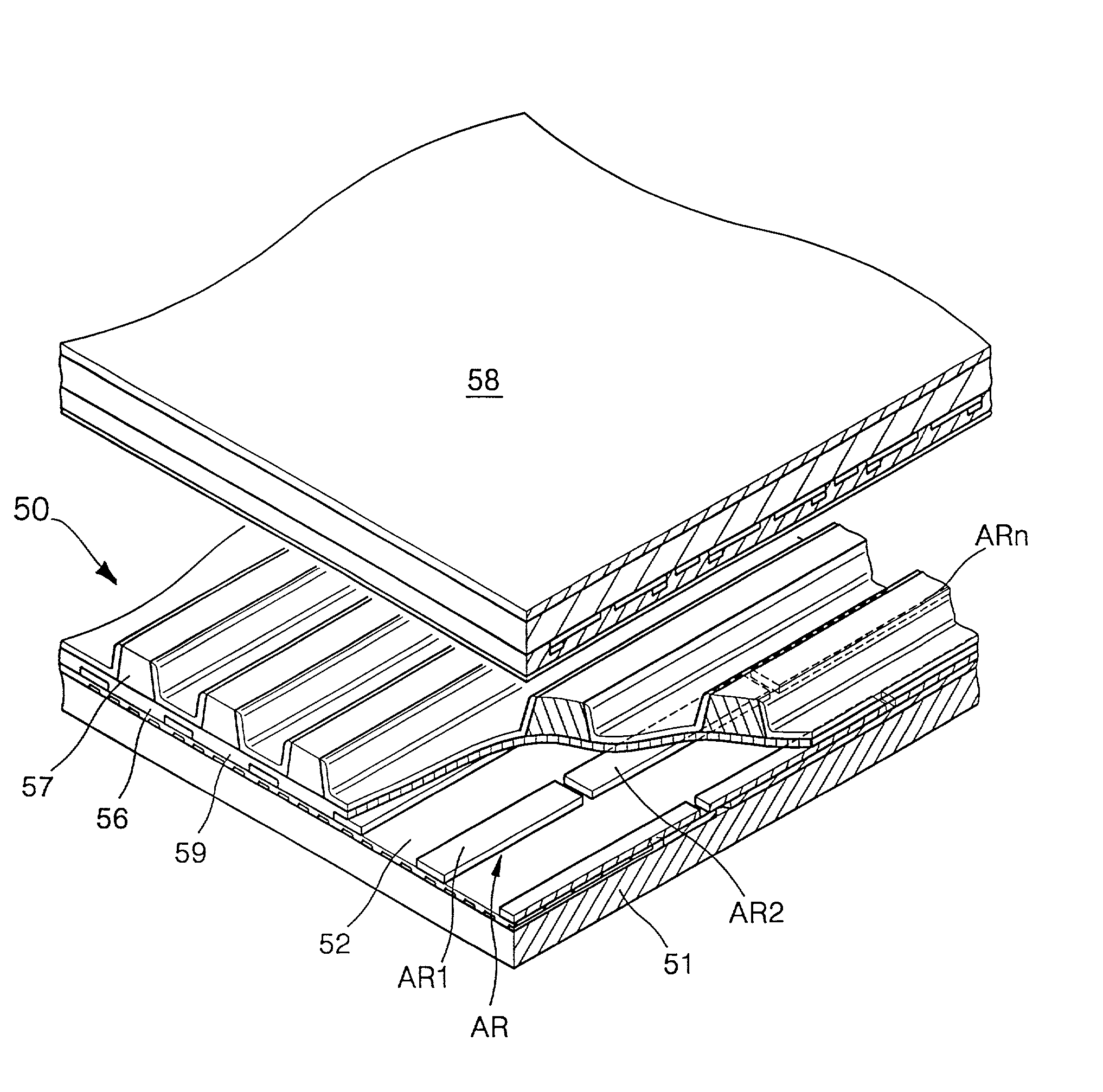
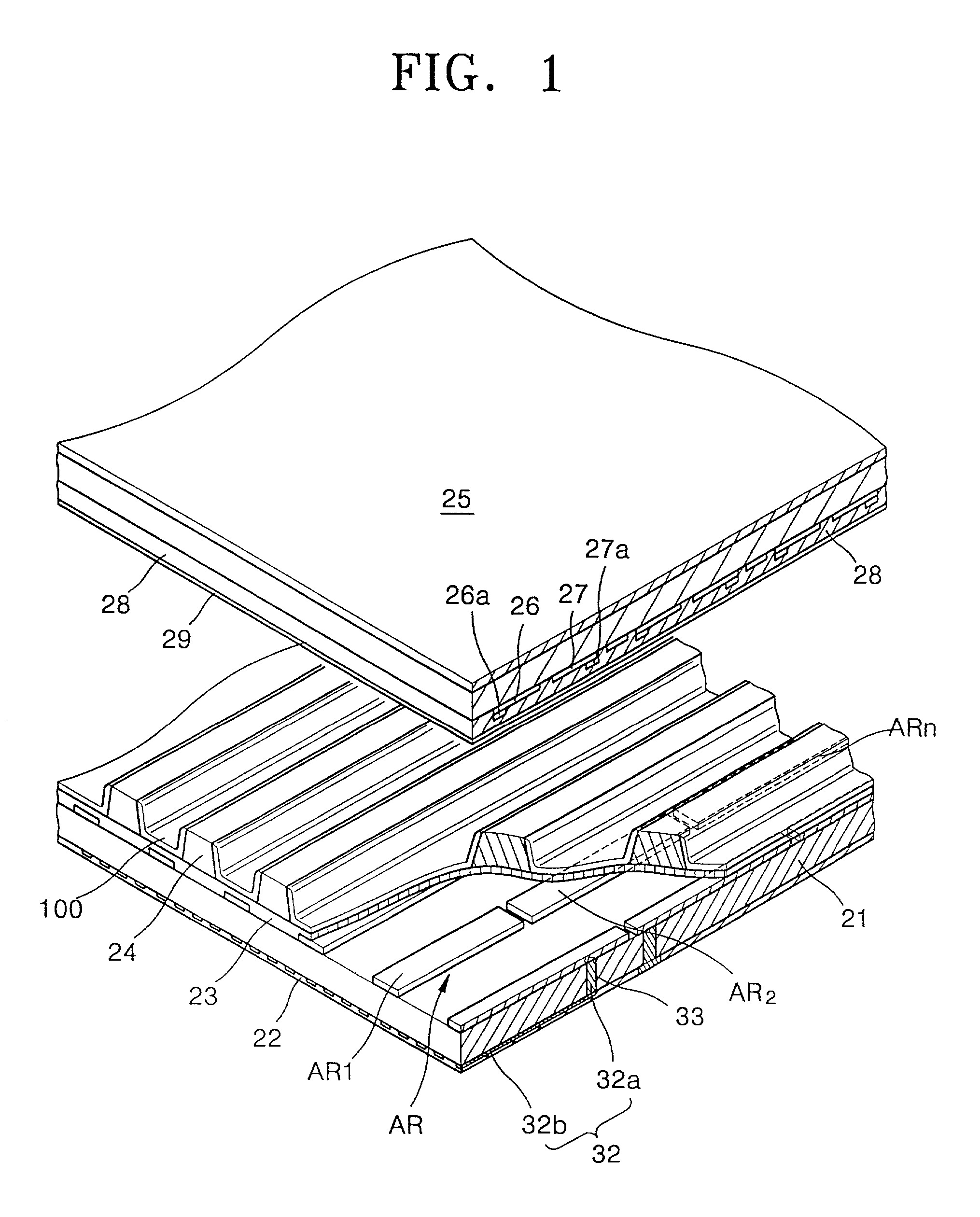
[0036] FIG. 1 is an exploded perspective view of a plasma display panel, in accordance with the principles of the present invention. FIG. 2 is a plan view showing the arrangement of the address electrodes of FIG. 1. FIG. 3 is a cross-sectional view of the substrate shown in FIG. 1.

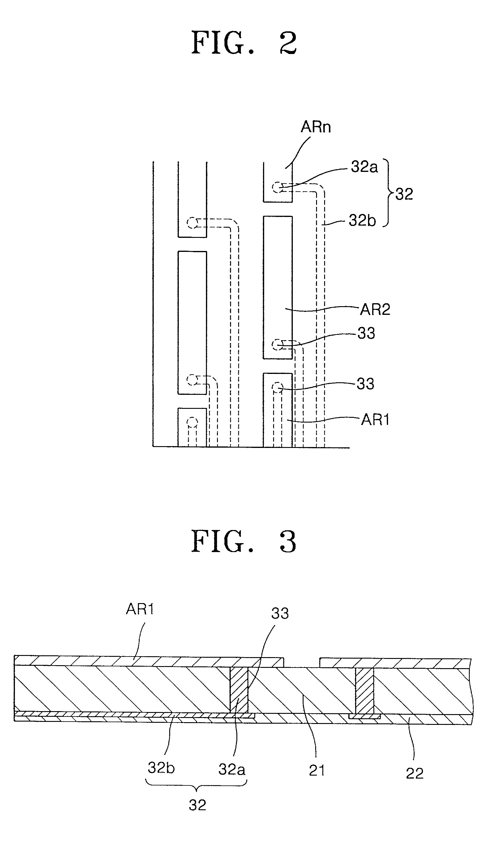
[0037] FIGS. 1 through 3 show a plasma display panel (PDP) according to an embodiment of the present invention. Address electrode lines AR have a predetermined pattern and are formed on an upper surface of a substrate 21. Each of the address electrode lines AR is split into at least three parts AR1-ARn lengthwise. Each of the split address electrode parts AR1-ARn has a length corresponding to at least two pixels. A predetermined current is applied to the split address electrode parts AR1-ARn by a voltage supplying unit.

[0038] The voltage supplying unit includes via holes 33 formed on areas of the substrate 21 corresponding to the respective split address electrode parts AR1-ARn, and an interconnection laye...

second embodiment

[0039] FIG. 4 is an exploded perspective view of a plasma display panel, in accordance with the principles of the present invention. FIG. 5 is a cross-sectional view of the substrate shown in FIG. 4.

[0040] As shown in FIGS. 4 and 5, the voltage supplying unit according to another embodiment of the present invention includes via holes 43 formed on a substrate 31 corresponding to the split address electrode parts AR1-ARn. Connecting portions 42 filled with conductive materials are formed in the via holes 43. Terminal patterns 43a connected to the respective connecting portions 42 are formed on a rear surface of the substrate 31 having the via holes 43. The terminal patterns 43a contact main terminal patterns 44a on a printed circuit board (PCB) 44 that is sealed with the substrate 31. Here, the main terminal patterns 44a are arranged on one surface of the PCB 44 in a same pattern as the terminal patterns 43a.

[0041] Referring to FIG. 1, a first dielectric layer 23 is formed on the subs...


PUM


Abstract

A plasma display panel including a substrate having via holes, partitions spaced a predetermined distance apart on the substrate, address electrodes having a predetermined pattern on portions of the substrate between adjacent pairs of the partitions, each address electrode being split into at least three parts with each split part corresponding to two pixels, a first dielectric layer on the substrate to cover the address electrodes and where the via holes correspond to the address electrodes, a conductive layer in the via holes and electrically connected with the address electrodes, terminals connected to the conductive layer on the rear surface of the substrate, a transparent front plate disposed opposite the substrate, sustaining electrodes on the front plate at a predetermined angle with respect to a direction of the address electrodes, the sustaining electrodes comprising pairs of first and second electrodes, and a second dielectric layer on the front plate to cover the sustaining electrodes.

Description

CLAIM OF PRIORITY[0001] This application makes reference to, incorporates the same herein, and claims all benefits accruing under 35 U.S.C. .sctn.119 from an application for PLASMA DISPLAY DEVICE earlier filed in the Korean Industrial Property Office on Mar. 13, 2001, and there duly assigned Serial No. 12892 / 2001 by that Office.BACKGROUND OF THE INVENTION[0002] 1. Technical Field[0003] The present invention relates to a plasma display panel (PDP) and, more particularly, to a plasma display panel having improved address electrodes.[0004] 2. Related Art[0005] A plasma display panel generates light by exciting fluorescent materials or special discharge gases. A predetermined voltage is applied between two electrodes to cause a discharge, and a fluorescent layer is excited by ultraviolet light generated by the discharge, thereby forming a picture image.[0006] A plasma display panel is a thin display device that can display images rapidly and that can allow for a large screen size. Plasm...

Claims


Application Information

Patent Timeline
Patent Type & Authority Applications(United States)
IPC IPC(8): H01J11/12H01J11/46
CPCH01J11/12H01J11/46H01J11/24H01J11/26H01J11/38
Inventor JEONG, JAE-SEOKHONG, DAE-YOUNG
Owner SAMSUNG SDI CO LTD
Why Eureka
Try Eureka