Integrated optical circuit device and method for producing the same

Inactive Publication Date: 2002-10-24
SHARP KK
View PDF0 Cites 26 Cited by
  • Summary
  • Abstract
  • Description
  • Claims
  • Application Information

AI Technical Summary

Benefits of technology

0033] Furthermore, all the optical elements according to the present invention can be produced through the same process. Therefore, the relative positioning of the optical elements is facilitated without misalignment along the height direction. Hence, the coupling efficiency is not degraded even in the case of poor processing accuracy.
0034] In the fabrication of the integrated optical circuit device according to the present invention, the formation of a lower electrode of the semiconductor laser section and the formation of a ridge of the optical waveguide section can be performed

Problems solved by technology

However, the hybrid method requires very accurate positioning and therefore is not highly industrially applicable, i.e., is not highly adaptable to being efficiently produced.
However, the structure shown in FIG. 14 inevitably results in the formation of a section 9 between the active layer 2 and the optical waveguide layer 6 which lacks the function of light confinement in a vertical direction.
Furthermore, since the active layer 2 and the optical waveguide layer 6 are formed through separate growth

Method used


Image

  • Integrated optical circuit device and method for producing the same
  • Integrated optical circuit device and method for producing the same
  • Integrated optical circuit device and method for producing the same

Examples


example 2

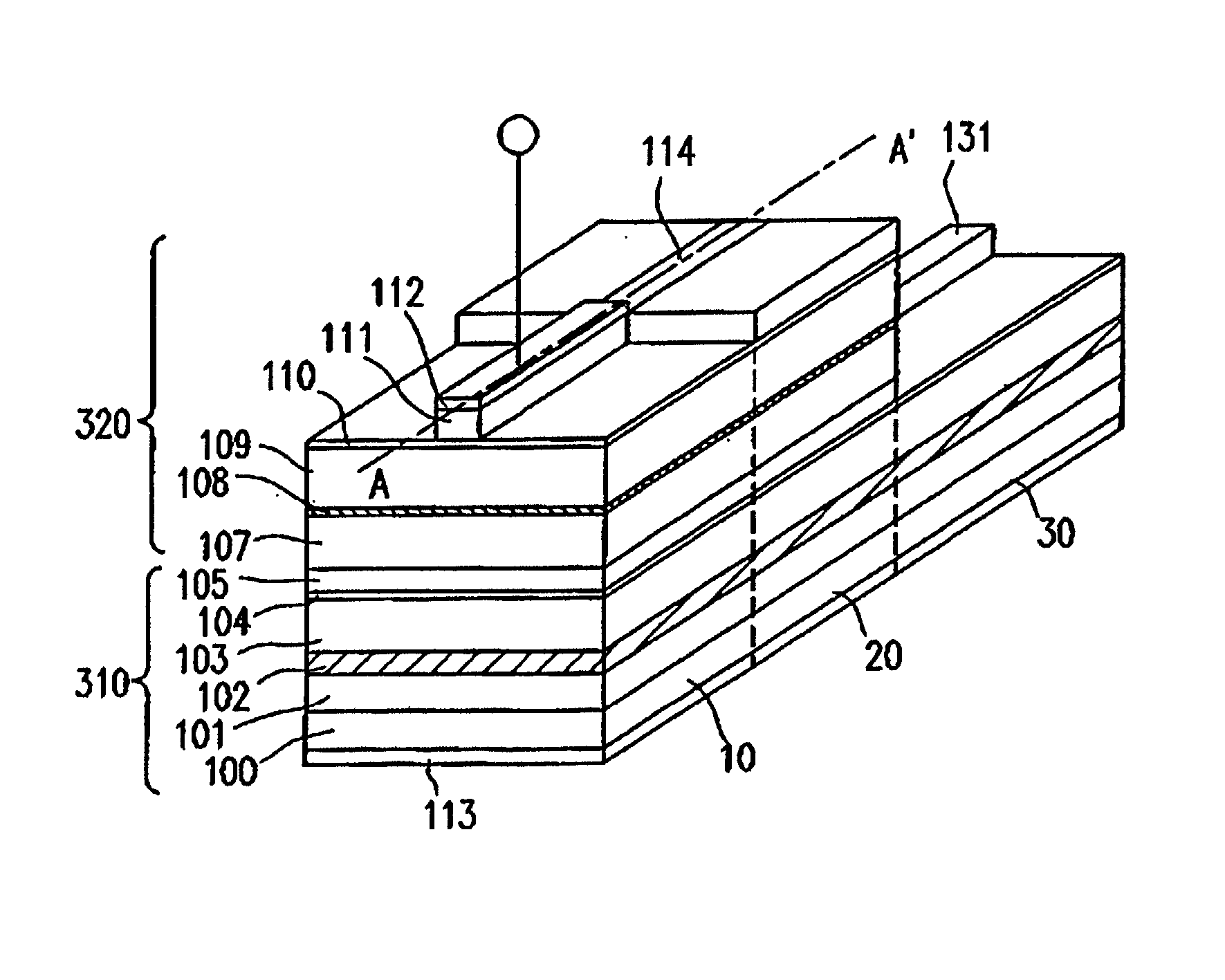
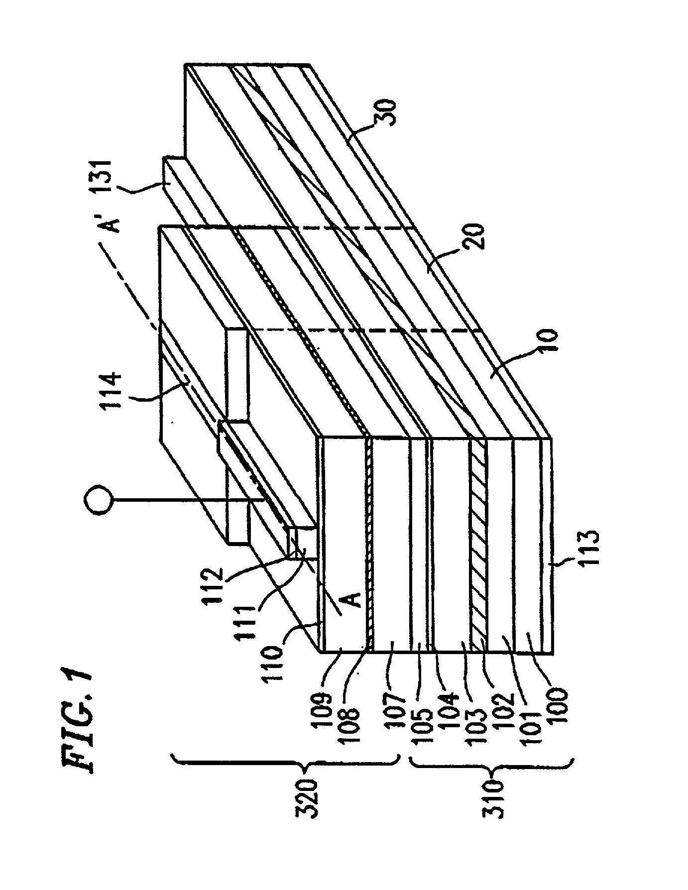
[0083] Example 2 of the present invention will be described with reference to FIG. 3. Specifically, the integrated optical conversion element according to the present example is a mode conversion type laser element which provides for the integration of optical circuit elements with optical coupling at low losses.

[0084] In FIG. 3, the constituent elements which also appear in FIG. 1 are denoted by like numerals.

[0085] First, a method for producing the integrated optical circuit device will be described. As in Example 1, in order to form an optical waveguide, an Al.sub.0.22Ga.sub.0.78As first optical guide layer 101, an Al.sub.0.20Ga.sub.0.80As optical waveguide layer 102 (thickness: 2 .mu.m), an Al.sub.0.22Ga.sub.0.78As second optical guide layer 103, an Al.sub.0.8Ga.sub.0.2As etching stopper layer 104, and an Al.sub.0.22Ga.sub.0.7As third optical guide layer 105 are layered on a GaAs substrate 100 in this order, by using a usual MOCVD method. These layers are formed as undoped layer...

example 3

[0099] An integrated optical circuit device according to Example 3 of the present invention will be described with reference to FIG. 6. Specifically, the integrated optical conversion element according to the present example is a mode conversion type laser element which achieves light distribution conversion along the transverse direction in addition to the light distribution conversion along the vertical direction achieved in Examples 1 and 2.

[0100] In FIG. 6, the constituent elements which also appear in FIG. 3 are denoted by like numerals, and the descriptions thereof are omitted. The process of producing the integrated optical circuit device of the present example is the same as the process described in Example 2.

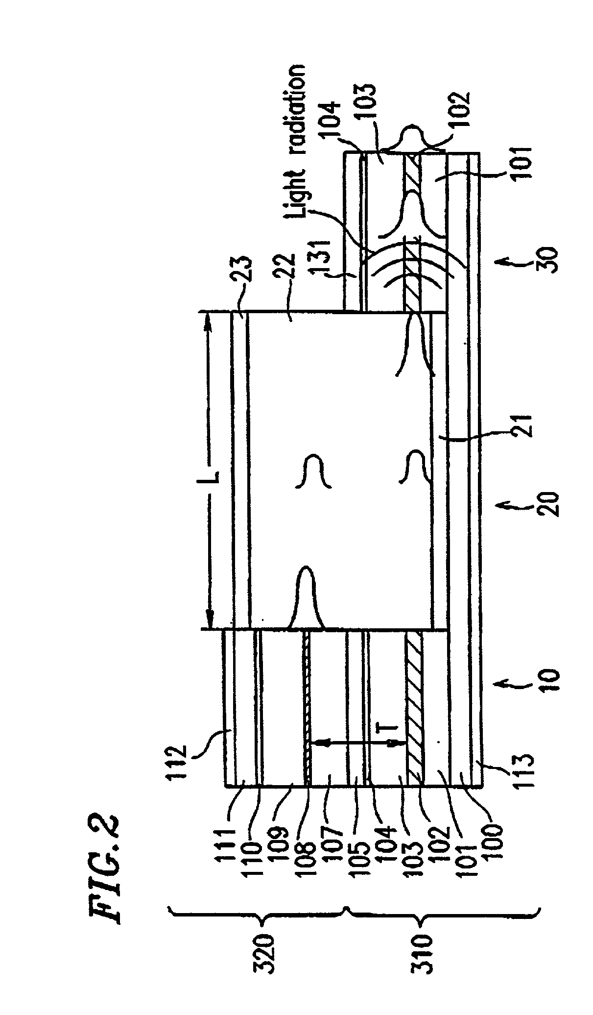
[0101] In the present example, the multimode interference region 20 has a depth of 4.75 .mu.m, a length of 200 .mu.m, and its buried portion 114 has a gradually varying width between 2 .mu.m (at an end face adjoining the semiconductor laser section 10) and 0.5 .mu.m (at...

example 4

[0109] An integrated optical circuit device according to Example 4 of the present invention will be described with reference to FIG. 7.

[0110] In FIG. 7, the constituent elements which also appear in FIG. 3 are denoted by like numerals, and the description thereof is omitted. The process of producing the integrated optical circuit device of the present example is basically the same as the process described in Example 2 except that a buried portion 114 of the multimode interference region 20 is formed so as to be as wide as 15 .mu.m according to the present example. The center line of the ridge 111 of the semiconductor laser section 10 and the center line of the ridge 131 of the optical waveguide section 30 are arranged so as to have an offset of 6.3 .mu.m along the width direction, and are located in line symmetry with respect to the center of the transverse direction of the multimode interference region 20.

[0111] Hereinafter, the functions of the integrated optical circuit device ac...


PUM


Abstract

An integrated optical circuit device includes: a first optical element section including first and second element regions deposited along a thickness direction; a second optical element section formed away from the first optical element section; and a multimode interference region provided between the first and second optical element sections, the multimode interference region including a buried portion formed along a light propagation direction. The first and second optical element sections are optically coupled to each other via the multimode interference region.

Description

[0001] 1. Field of the Invention[0002] The present invention relates to an integrated optical circuit device and a method for producing the same, and more specifically, to a method for coupling a plurality of optical elements. In particular, the present invention relates to an integrated. optical circuit device incorporating a semiconductor laser section and an optical waveguide section having different near fields from each other, as well as a method for producing the same,[0003] 2. Description of the Related Art[0004] Conventionally, integrated optical circuit device incorporating a semiconductor laser element (also referred to as the "semiconductor laser section") and an optical waveguide element (also referred to as the "optical waveguide section") having different near fields from each other are produced by a hybrid method which involves separately fabricating a semiconductor laser. element and an optical waveguide element having different near fields and then combining the two...

Claims


Application Information

Patent Timeline
IPC IPC(8): G02B6/12G02B6/122G02B6/28H01S3/08H01S5/026H01S5/10H01S5/323
CPCG02B6/122G02B6/2813G02B2006/12078G02B2006/12092H01S5/32316G02B2006/121G02B2006/12178H01S5/026H01S5/1032G02B2006/12097
Inventor SHIMONAKA, ATSUSHIKAWANISHI, HIDENORI
Owner SHARP KK
Why Eureka
Try Eureka