Method and apparatus for multiple byte or page mode programming and reading and for erasing of a flash memory array

a flash memory array and programming and reading technology, applied in the field of semiconductor memory, can solve the problems of increasing the size of the memory chip, and slow programming using the fn tunneling from the drain edge to the floating ga

Inactive Publication Date: 2002-11-14
WINBOND ELECTRONICS CORP
View PDF9 Cites 104 Cited by
  • Summary
  • Abstract
  • Description
  • Claims
  • Application Information

AI Technical Summary

Problems solved by technology

Unfortunately, programming using FN tunneling from the drain edge to the floating gate is relatively slow.
Transistors using FN programming generally requires a longer channel length, leading to larger cell size.
FN programmed memories also require bit-latch circuitry, which increases the size of the memory chip.
Unfortunately, the high drain voltage and programming current required by CHE renders the technique disadvantageous for use in low power applications, and severely limits the number of bits that can be programmed at one time.
Simultaneous multiple byte programming is difficult to perform, as a practical matter.
While multiple byte programming and page mode programming of a CHE type memory can be achieved by repeated programming groups of bits until the desired amount of memory is programmed, the approach can result in an unfavorable condition known as program-disturb.
A similar problem occurs during read-out of data.
While program-disturb and read-disturb can be avoided by the use of an isolating select transistor in each memory cell, such transistors are undesirable insofar as they cause an increase in the size of the memory cell and a corresponding decrease in the memory array density.
However, simultaneous multiple byte programming and page mode programming are still difficult to achieve.
Unfortunately, as in the case the CHE memory array, the use of isolating select transistors in CISEI memory cells increases their size, and the technique of repeated programming groups of bits until the desired amount of memory is programmed can cause program-disturb.
While CHE and CISEI cell programming is faster that FN cell programming, multiple byte programming and page mode programming of CHE and CISEI memory arrays remains problematical.
We have found that flash memory suffers disturbance of the floating gate potential especially during page mode programming operations, and may also suffer disturbance of the floating gate potential during read operations.

Method used


Image

  • Method and apparatus for multiple byte or page mode programming and reading and for erasing of a flash memory array
  • Method and apparatus for multiple byte or page mode programming and reading and for erasing of a flash memory array
  • Method and apparatus for multiple byte or page mode programming and reading and for erasing of a flash memory array

Examples


Embodiment Construction

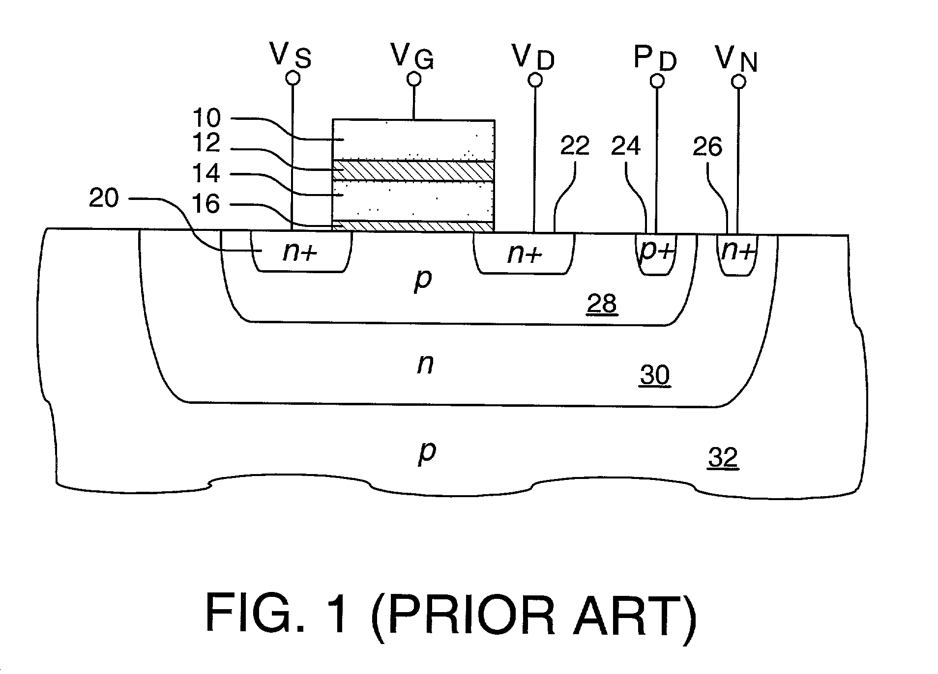
[0034] EEPROM cells of the stacked gate type shown in FIG. 1 are used in a variety of different types of flash array architectures where they are subject to disturbance of the floating gate potential during CHE page mode programming operations, and may also suffer disturbance of the floating gate potential during read operations.

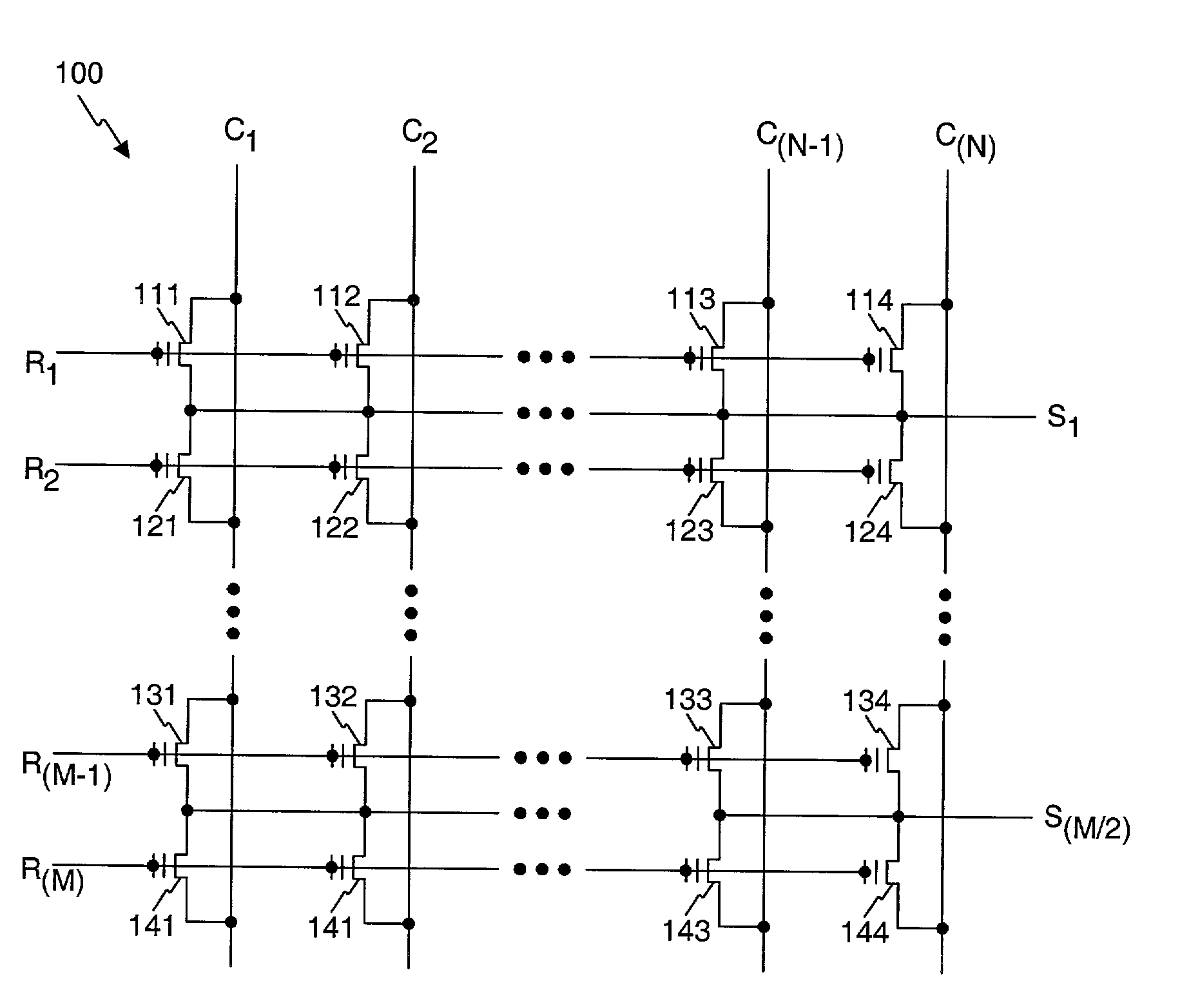
[0035] A common ground NOR array 100 is shown in FIG. 3. Simplified for clarity, the array 100 illustratively is arranged in M rows and N columns of memory cells, and each individual memory cell 111-114, 121-124, 131-134 and 141-144 is a stacked gate type of cell such as that shown in FIG. 1 but preferably having a halo implant in a manner well known in the art. While a variety of other type of nonvolatile memory cells using floating gates and other classes of nonvolatile memory cells using charge trapping like the MNOS (Metal-Nitride-Oxide-Semiconductor) device to set the threshold voltage V.sub.T of the cell may also be used, the use of the stacked gate ty...


PUM


Abstract

A memory array contains memory cells designed to be erased using Fowler-Nordheim ("FN") tunneling through the channel area, and programmed using either channel hot electron injection ("CHE") or channel-initiated secondary electron injection ("CISEI"). To reduce disturbance of the floating gate potential of unselected memory cells during programming operations and read operations, the unselected word lines are brought to a negative potential rather than ground potential. To reduce disturbance of the floating gate potential of unselected memory cells during FN erase operations, the unselected word lines are brought to a positive potential rather than ground potential.

Description

[0001] This application claims the benefit of U.S. Provisional Patent Application No. 60 / 291,156, filed May 14, 2001 (Hsia et al., "Apparatus and method for multiple byte or page mode programming or erasure in a nonvolatile flash memory array," Attorney Docket No. 11030.00), which is hereby incorporated herein by reference in its entirety.[0002] 2. Field of the Invention[0003] The present invention relates to semiconductor memory, and more particularly to nonvolatile semiconductor memory that is programmable as well as erasable.[0004] 2. Description of the Related Art[0005] Nonvolatile memory retains stored data when power is removed, which is required or at least highly desirable in many different types of computers and other electronic devices. Some types of nonvolatile memory are capable of being repeatedly programmed and erased, including erasable programmable read only semiconductor memory generally known as EPROM, and electrically erasable programmable read only semiconductor ...

Claims


Application Information

Patent Timeline
Patent Type & Authority Applications(United States)
IPC IPC(8): G11C16/10G11C16/16G11C16/34
CPCG11C16/10G11C16/3418G11C16/16
Inventor HAN, KYUNG JOONTRAN, DUNGLONGCOR, STEVEN W.HSIA, STEVE K.
Owner WINBOND ELECTRONICS CORP
Why Eureka
Try Eureka