Paek embossing and adhesion for microfluidic devices

a technology of microfluidic devices and adhesives, which is applied in the direction of cellulose adhesives, fluid speed measurement, chemical vapor deposition coatings, etc., can solve the problems of high cost of melt-processing equipment and tools necessary to process paek, interfering moieties such as salts are washed away, and the manufacturing challenges of paek thermoplastic materials are difficul

Inactive Publication Date: 2003-01-23
AGILENT TECH INC
View PDF6 Cites 43 Cited by
  • Summary
  • Abstract
  • Description
  • Claims
  • Application Information

AI Technical Summary

Problems solved by technology

As a result, interfering moieties such as salts are washed away.
Although PEEK is mentioned in Myers as a possible substrate material, in practice, PAEK thermoplastic materials have presented difficult manufacturing challenges.
One challenge has been that the melt-processing equipment and tools necessary to process PAEK are expensive due to the fact that PAEK is a high-temperature melting engineering thermoplastic.
Moreover, the high melting point temperature (T.sub.m) of PAEK has also made it difficult to optimize the process conditions.
In addition, traditional bonding materials used for PAEK devices, such as epoxides and acrylates, are not chemically inert to the solvents and temperatures that are commonly required in microfluidic applications, such as High Performance Liquid Chromatography (HPLC).
Such traditional adhesive agents are not sufficiently resistant to solvents, such as methyl sulfoxide (DMSO), dimethyl formamide (DMF) and N-methyl pyrrolidone (NMP).
Therefore, it has been difficult to bond PAEK to PAEK and PAEK to other materials.

Method used


Image

  • Paek embossing and adhesion for microfluidic devices
  • Paek embossing and adhesion for microfluidic devices
  • Paek embossing and adhesion for microfluidic devices

Examples


Embodiment Construction

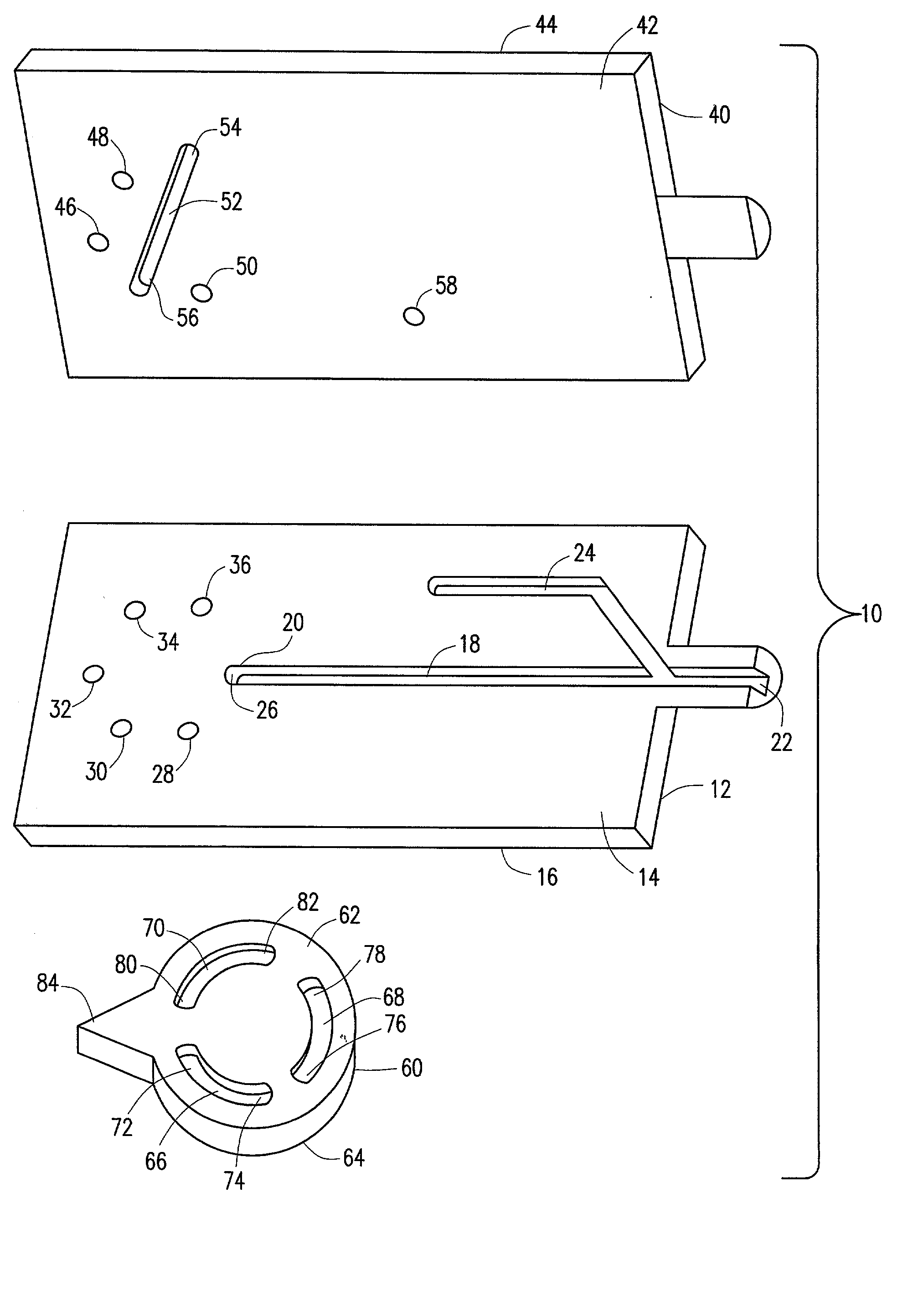
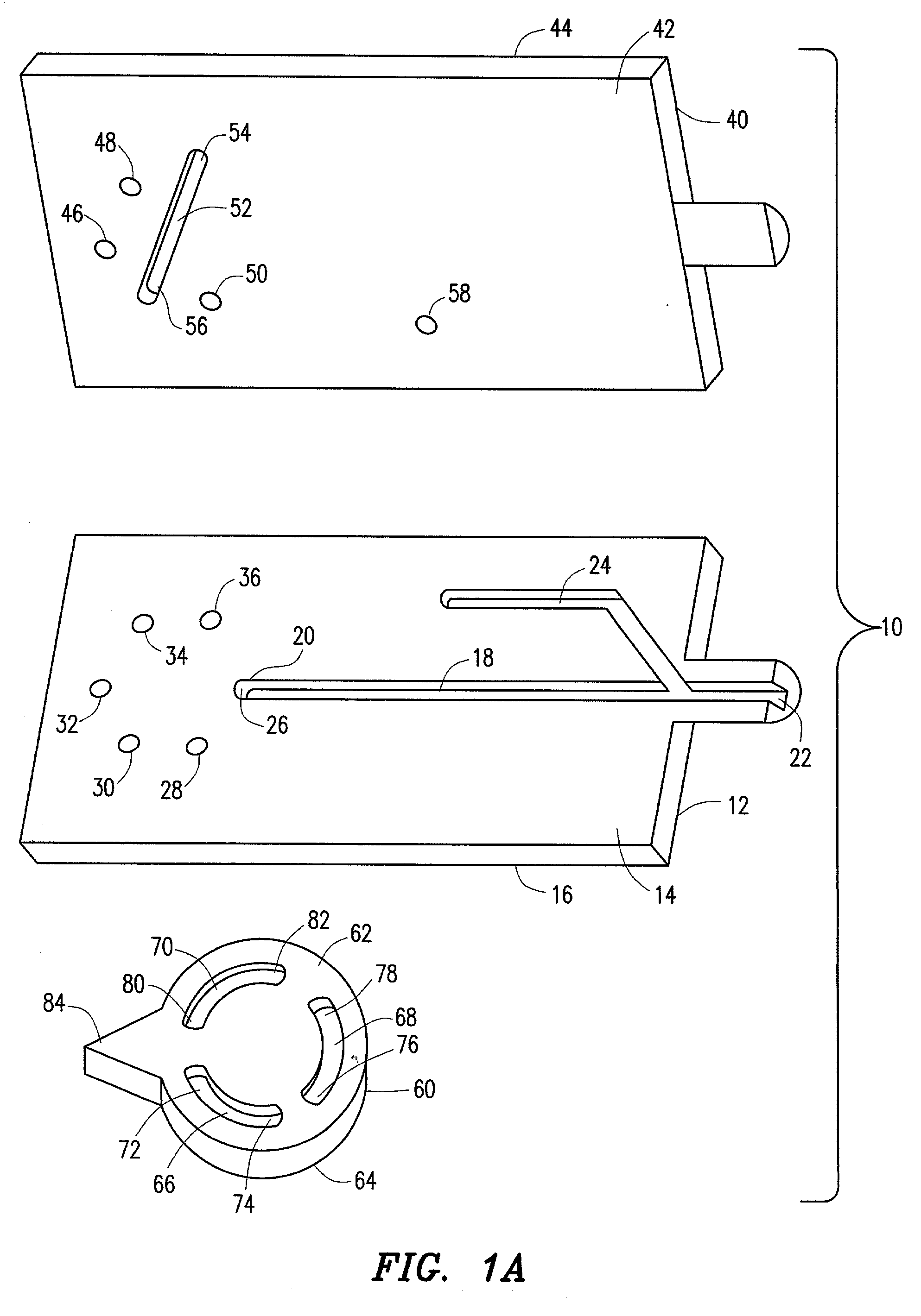
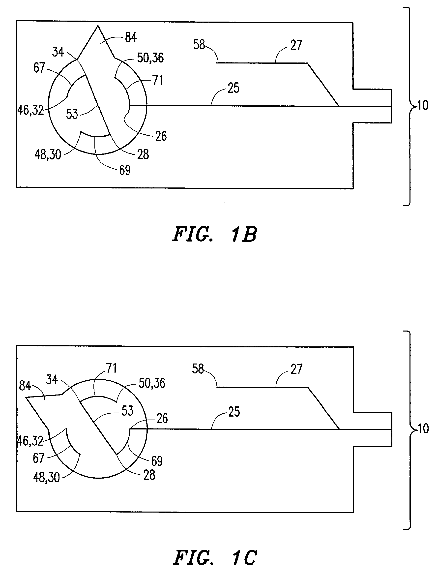
[0031] The numerous innovative teachings of the present application will be described with particular reference to the exemplary embodiments. However, it should be understood that these embodiments provide only a few examples of the many advantageous uses of the innovative teachings herein. In general, statements made in the specification do not necessarily delimit any of the various claimed inventions. Moreover, some statements may apply to some inventive features, but not to others.

[0032] It must be noted that, as used in the specification and the appended claims, the singular forms "a," "an" and "the" include plural referents unless the context clearly dictates otherwise. Thus, for example, reference to "a mechanical" includes a plurality of microchannels, reference to "a fluid" includes a mixture of fluids, reference to "a component property" includes a plurality of component properties and the like.

[0033] In this specification and in the claims that follow, reference will be ma...


PUM

PropertyMeasurementUnit
thicknessaaaaaaaaaa
thicknessaaaaaaaaaa
thickaaaaaaaaaa

Abstract

A fabrication and adhesion method for a polyaryl-ether-ketone (PAEK) device, such as a microfluidic device, is disclosed. At least one glassy uncrystallized PAEK substrate is heated up to near or above the glass transition temperature to allow the substrate to crystallize from the glass state, while embossing the substrate with patterns. Bonding the PAEK substrate to another substrate is accomplished using a solvent-resistant adhesive, such as a polyimide-based adhesive, in combination with an adhesion enhancement treatment. In certain embodiments, the adhesion enhancement treatment is a plasma treatment or a chemical sulfonation treatment.

Description

[0001] This U.S. Nonprovisional Application for Patent is a Continuation-in-Part of U.S. Nonprovisional application for patent Ser. No. 09 / 908,231, which was filed on Jul. 17, 2001. U.S. Nonprovisional application for patent Ser. No. 09 / 908,231 is also hereby incorporated by reference in its entirety herein.[0002] 1. Technical Field of the Invention[0003] The present invention relates generally to microfluidic devices, and particularly to fabrication and adhesion of microfluidic devices.[0004] 2. Description of Related Art[0005] In recent years, microfluidic device technologies, also referred to as microfluidics and Lab-on-a-Chip technologies, have been proposed for a number of applications, including chemical analysis for pharma, biotechnology, fuel cells, etc. Microfluidic devices hold great promise for many applications, particularly in applications that employ rare or expensive fluids, such as proteomics and genomics. The small size of the microfluidic devices allows for the ana...

Claims


Application Information

Patent Timeline
Patent Type & Authority Applications(United States)
IPC IPC(8): B01L3/00B29C43/56B29C59/02B29C59/14B29C65/00B29C65/48B81B1/00B81C1/00G01N27/447G01N30/60
CPCB01L3/502707Y10T428/24479B01L3/502738B01L2200/0689B01L2200/12B01L2300/123B01L2400/0622B01L2400/0644B29C43/56B29C59/02B29C59/14B29C59/142B29C65/521B29C66/001B29C66/02B29C66/026B29C66/54B29C66/7465B29C66/82661B29C66/91941B29C66/91943B29C2071/022B29K2071/00B29K2079/08B29K2309/08B29K2995/0039B29K2995/0041B29L2031/756B81B1/00B81C1/00357B81C2201/019G01N27/44791G01N30/60G01N30/6052G01N30/6095B01L3/502715Y10T156/1023B29C66/91411B29C66/91445B29C66/53461B29C66/536B29C65/4835B29C65/48B29C66/919B29C66/9192B29C66/73115B29C66/73117B29C65/00B29C66/73771B29C66/73775B29C66/73921B29C66/73941B29C66/73772B29C66/73776B29C66/73774B29C66/71B29C66/1122
Inventor ROITMAN, DANIEL B.KILLEEN, KEVIN P.SEAWARD, KAREN L.YIN, HONGFENGROBOTTI, KARLA
Owner AGILENT TECH INC
Why Eureka
Try Eureka