

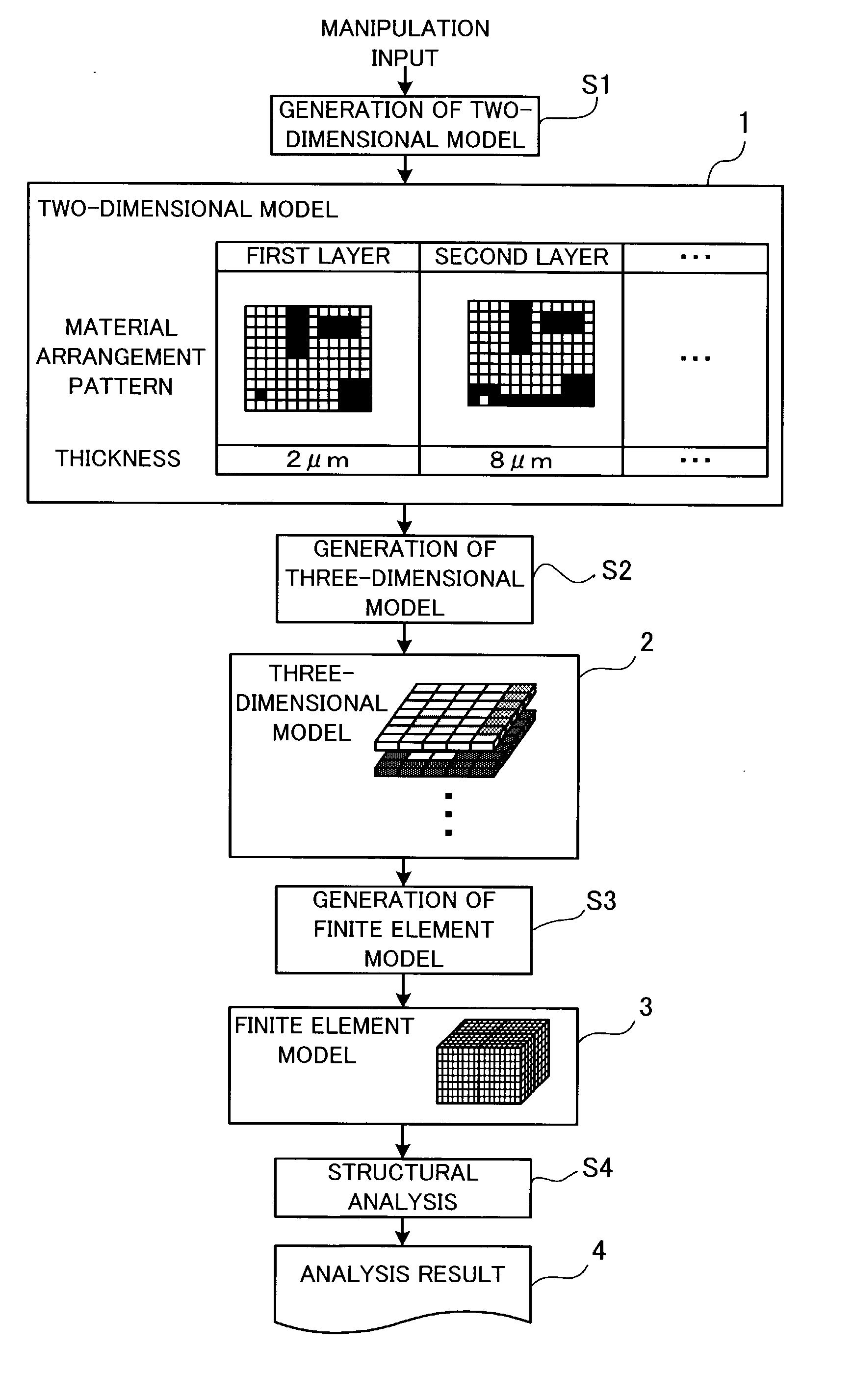
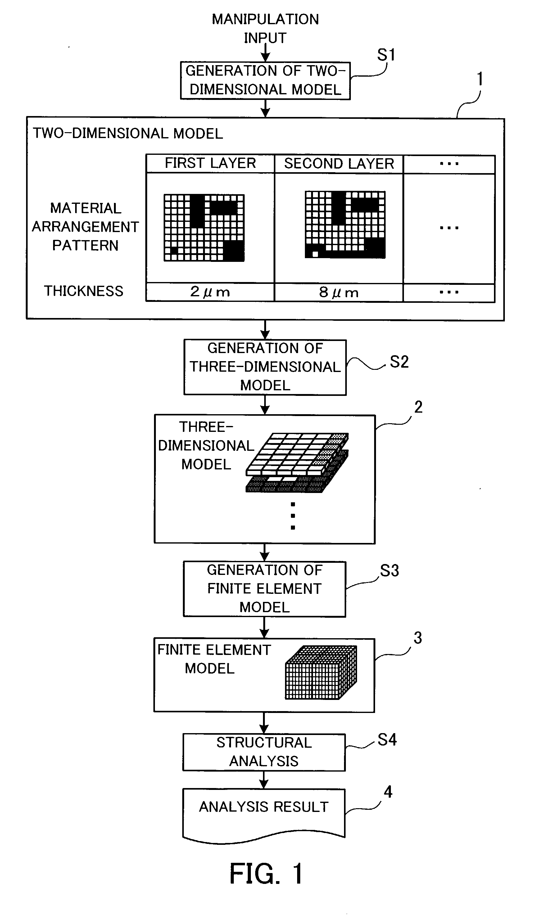
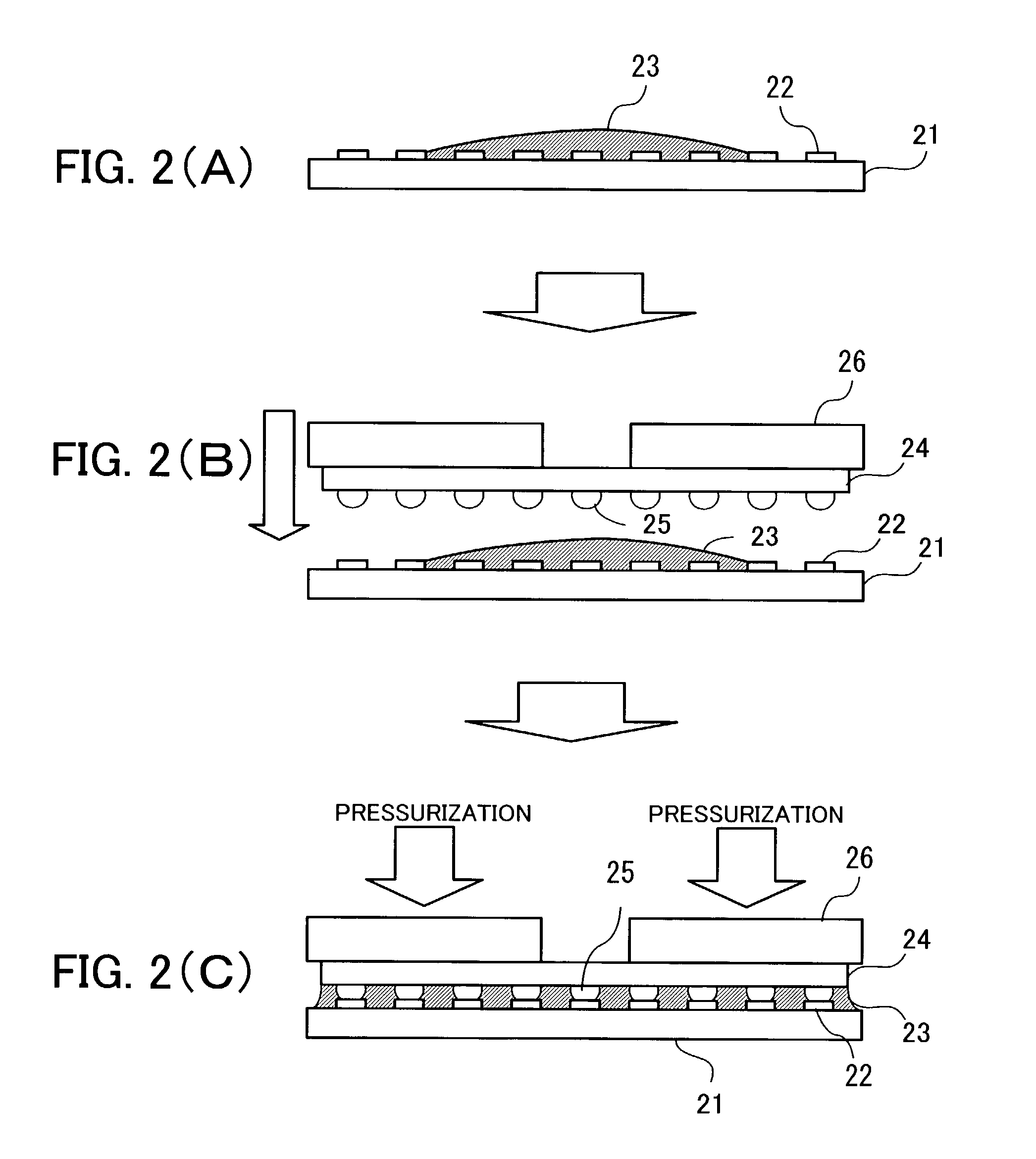
Structural analysis program, a structural analysis method, a structural analysis apparatus, and a production process of a semiconductor integrated circuit
- Summary
- Abstract
- Description
- Claims
- Application Information
AI Technical Summary
Benefits of technology
Problems solved by technology
Method used
Image

Examples
Embodiment Construction
[0348] The processing functions indicated in the first and second embodiments can be realized by computers. In this case, programs which describe details of processing realizing the functions which the structural analysis apparatus, the circuit design apparatus, and the production control apparatus should have are provided. When the computers execute the programs, the above processing functions are realized on the computers. The programs describing the details of processing can be stored in a computer-readable storage mediums. The computer-readable storage mediums may be a magnetic storage device, an optical disk, an optical magnetic recording medium, a semiconductor memory, or the like. The magnetic storage device may be a hard disk device (HDD), a flexible disk (FD), a magnetic tape, or the like. The optical disk may be a DVD (Digital Versatile Disk), a DVD-RAM (Random Access Memory), a CD-ROM (Compact Disk Read Only Memory), a CD-R (Readable) / RW (ReWritable), or the like. The opt...
PUM
 Abstract
Description
Claims
Application Information