Modular thermoelectric couple and stack
a thermoelectric couple and module technology, applied in the direction of electrical equipment, semiconductor devices, semiconductor/solid-state device details, etc., can solve the problems of reducing operating efficiency, reducing overall cooling, and high cumulative heat resistance or impedance loss
- Summary
- Abstract
- Description
- Claims
- Application Information
AI Technical Summary
Problems solved by technology
Method used
Image
Examples
first embodiment
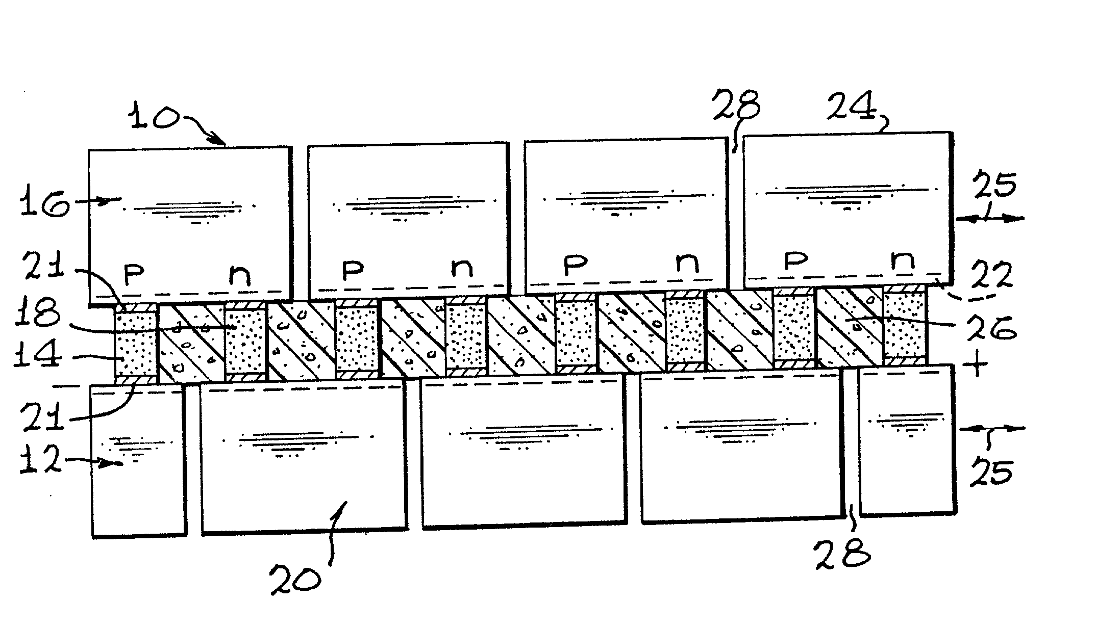
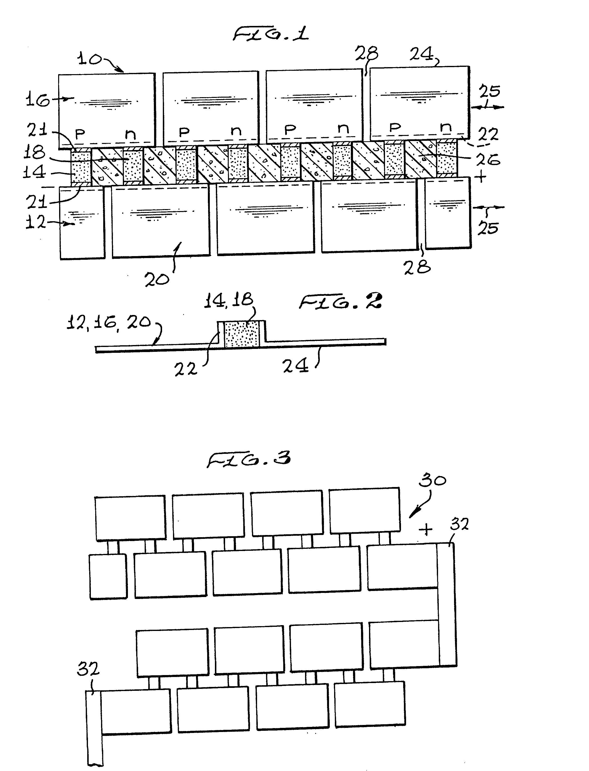
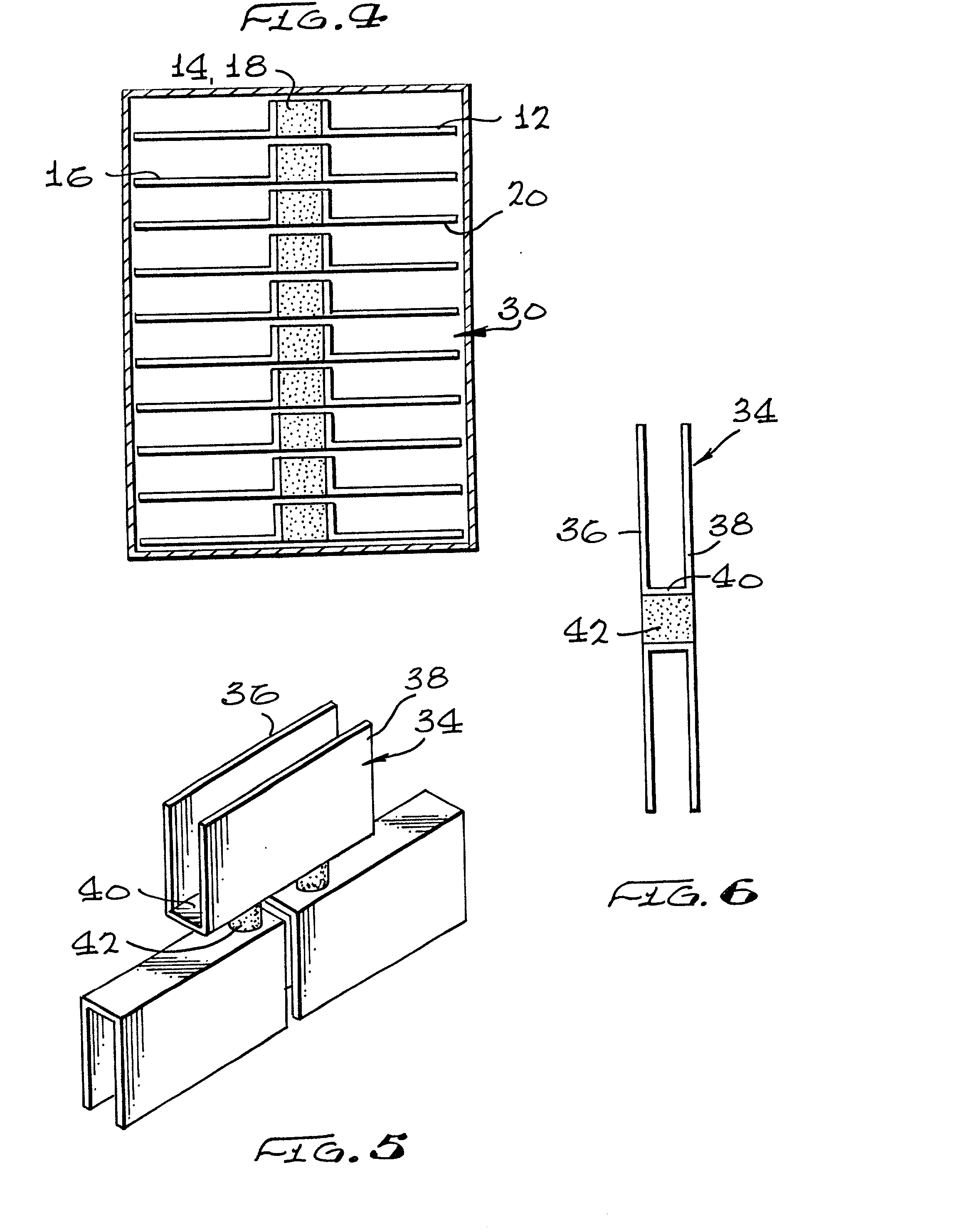
[0040] Turning now to the drawing and the invention, reference is made primarily to FIGS. 1 and 2. As shown there, a thermoelectric semiconductor couple of the invention is enumerated generally as 10 and includes a first electrode and heat transferring means 12, a quantity of a p-type thermoelectric semiconductor 14, a second electrode and heat transferring means 16, a quantity of an n-type thermoelectric semiconductor 18 and a third electrode and heat transferring means 20. Each of the electrodes and heat transferring means, as the name implies, is constructed of a good electrical conductor as well as a suitable material for transferring heat (e.g., to and from an ambient fluid). A suitable material for this purpose is a metal such as copper or aluminum. As indicated by the symbols "+" and "-", the means 12, 16 and 20 when connected with the semiconductor quantities 14 and 18 form an electrical series circuit via which the semiconductor quantities are energized to function thermoel...
third embodiment
[0047] For the ensuing description of the invention, reference is made to FIG. 7. This embodiment is especially advantageous in being able to be assembled directly onto a solid surface which may be either part of an object to be "cooled", for example, or a waste heat sink. As shown, four electrodes and heat transferring means 44, 46, 48 and 50 have four pairs of p-type and n-type thermoelectric semiconductor bodies or pellets 52 and 54, respectively secured thereto as in the first described embodiment. However, instead of a further set of electrodes and heat transferring means, pairs of p- and n-type semiconductors are serially electrically connected by a conductor 56 deposited on one surface of a dielectric segment 58 (e.g., ceramic), the opposite surface of which can be adhered in any desired manner (e.g., soldered) to any desired solid surface without interfering with the electric energization of the pellets.
[0048] FIG. 8 shows a prior art semiconductor module 60 composed of a nu...
fifth embodiment
[0053] For the ensuing detailed description of the invention reference is now made to FIGS. 14-16. First and second support plates 128 and 130, which may be of identical construction, include sets 132 of parallel slotted openings 134 of such relative spaced apart relation as to receive previously described fin / conductors 36,38 therethrough with the plates pressed against the module conductors. When so assembled, the plates 128 and 130 provide overall structural rigidity to the modules while, at the same time, establishing an air barrier between the "hot" and "cold" sides of the modules that limits convection into the space between the two plates.
[0054] In addition, it is preferable to provide an edge seal 136 such as an O-ring, for example, to reduce even further external convection air currents from moving into the space between the plates and into contact with the semiconductor pellets degrading system heat efficiency. This seal also prevents humid ambient air from making its way ...
PUM
 Abstract
Description
Claims
Application Information


