Active matrix type display device

a display device and active matrix technology, applied in the direction of static indicating devices, identification means, instruments, etc., can solve the problems of large area occupied by wiring in the region between rows, complex wiring undulation, and complicated wiring

Inactive Publication Date: 2003-04-10
SANYO ELECTRIC CO LTD
View PDF9 Cites 46 Cited by
  • Summary
  • Abstract
  • Description
  • Claims
  • Application Information

AI Technical Summary

Problems solved by technology

However, in an active matrix type organic EL display device, as shown in FIG. 1, a data line DL and a driving power supply line VL must be connected to each pixel in the column direction and, thus, when the delta arrangement is employed the wiring becomes more complicated than in a comparable LCD.
However, as is clear from FIG. 2, the wiring undulates in a complex manner among the rows and the area occupied by the wiring in the region between the rows is large.
When the area occupied by the wiring is large as in this case, the emission region (formation region of the organic EL element) is significantly limited on a substrate having a limited area, and, thus, improvements in aperture ratio cannot be achieved, that is, bright display cannot be produced.
Therefore, when the wiring resistance of the d

Method used


Image

  • Active matrix type display device
  • Active matrix type display device
  • Active matrix type display device

Examples


Embodiment Construction

[0036] The preferred embodiment of the present invention (hereinafter referred to simply as the "embodiment") will now be described referring to the drawings.

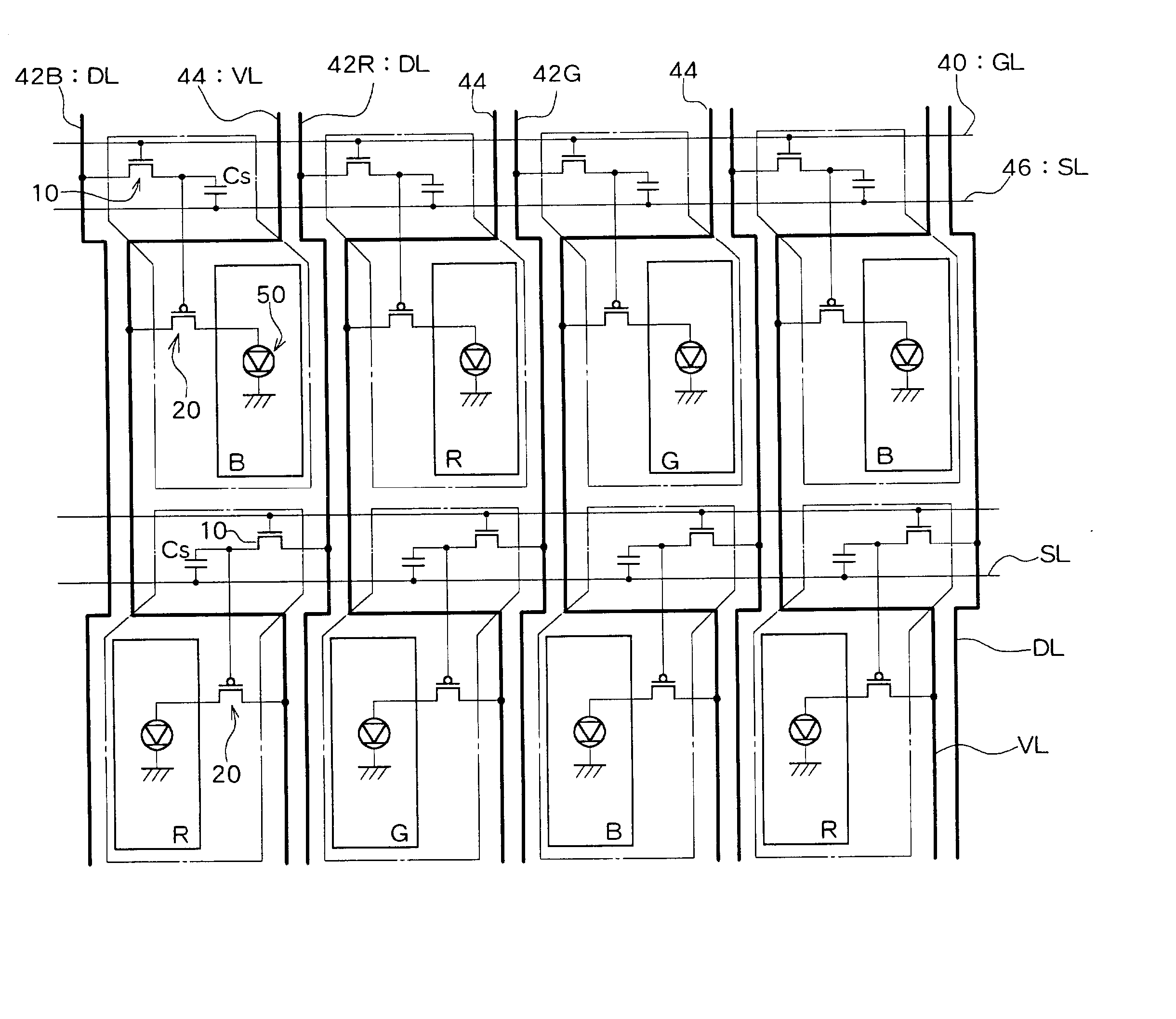
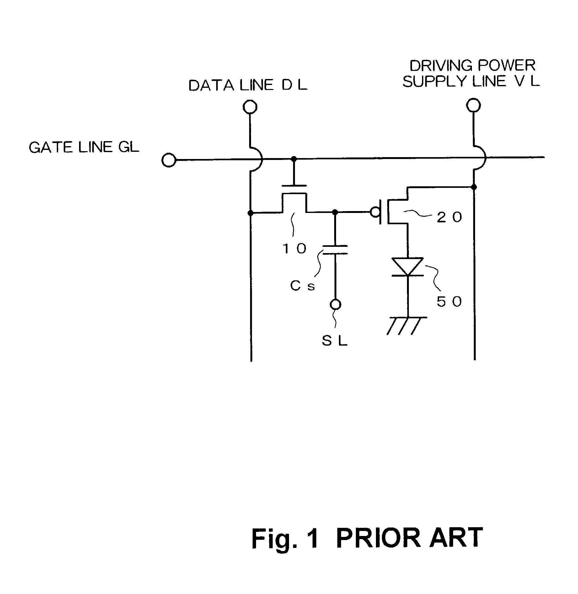
[0037] FIG. 3 shows a pixel layout of an active matrix type EL display device having m rows and n columns according to an embodiment of the present invention. A pixel is represented in FIG. 3 by a region surrounded by one-dotted chain lines. The circuit structure is identical to that shown in FIG. 1 and each pixel comprises an organic EL element 50 as an element to be driven, a switching TFT (first TFT) 10, an element driving TFT (second TFT) 20, and a storage capacitor Cs.

[0038] The gate of the first TFT 10 is connected to a gate line (GL) 40. In an n-channel (n-ch) first TFT 10, for example, a drain of the first TFT 10 is connected to a data line (DL) 42 and a source is connected to the storage capacitor Cs. The storage capacitor Cs comprises a first electrode which is integral with the source of the first TFT 10 and a second...


PUM


Abstract

An active matrix type display device comprising a plurality of pixels arranged in a matrix form, wherein each of the plurality of pixels comprises a display element, a second TFT for supplying power from a driving power supply line to the display element, and a first TFT for controlling the second TFT based on a data signal supplied from a data line when selected, and the driving power supply line extends across the pixel region. More specifically, of opposing first and second sides of a pixel, in a section where the first TFT is connected to the data line, the driving power supply line is placed on the second side, being the side opposite the data line, and in a section where the second TFT is connected to the driving power supply line, the driving power supply line is placed on the first side. In this manner, pixels provided in positions shifted for each row can be connected with a simple wiring layout.

Description

[0001] 1. Field of the Invention[0002] The present invention relates to an active matrix type display device, and in particular to a layout of pixels and wiring in such a device.[0003] 2. Description of the Related Art[0004] Electroluminescence (hereinafter referred to simply as "EL") display devices in which a self-illuminating EL element is used for each pixel have advantages such as thinness and low power consumption, in addition to being self-illuminating. Because of these advantages, EL display devices have currently attracted much attention as an alternative display device for liquid crystal display devices (LCDs) and CRTs, and effort is therefore now being expended on their development.[0005] In particular, an active matrix type EL display device in which a switching element for individually controlling an EL element such as a thin film transistor (TFT) is provided in each pixel so that the EL element is driven individually for each pixel is highly expected as a high-resoluti...

Claims


Application Information

Patent Timeline
IPC IPC(8): G09F9/00H01L51/50G09F9/30G09G3/20G09G3/30G09G3/32H01L21/77H01L27/12H01L27/32H05B33/00
CPCG09G3/3225G09G2300/0426G09G2300/0452G09G2300/0842H01L27/124H01L27/12H01L27/3211H01L27/3276G09G2320/0223H10K59/35H10K59/131H05B33/00
Inventor ANZAI, KATSUYA
Owner SANYO ELECTRIC CO LTD
Why Eureka
Try Eureka