

Interconnection structure with insulation comprising cavities
a technology of interconnection structure and cavity, which is applied in the manufacture of basic electric elements, electrical equipment, semiconductor/solid-state devices, etc., can solve the problems of unable to fill the gaps between the gaps, the problem of unable to produce expanded contacts, and the use of vacuum or air
- Summary
- Abstract
- Description
- Claims
- Application Information
AI Technical Summary
Problems solved by technology
Method used
Image

Examples
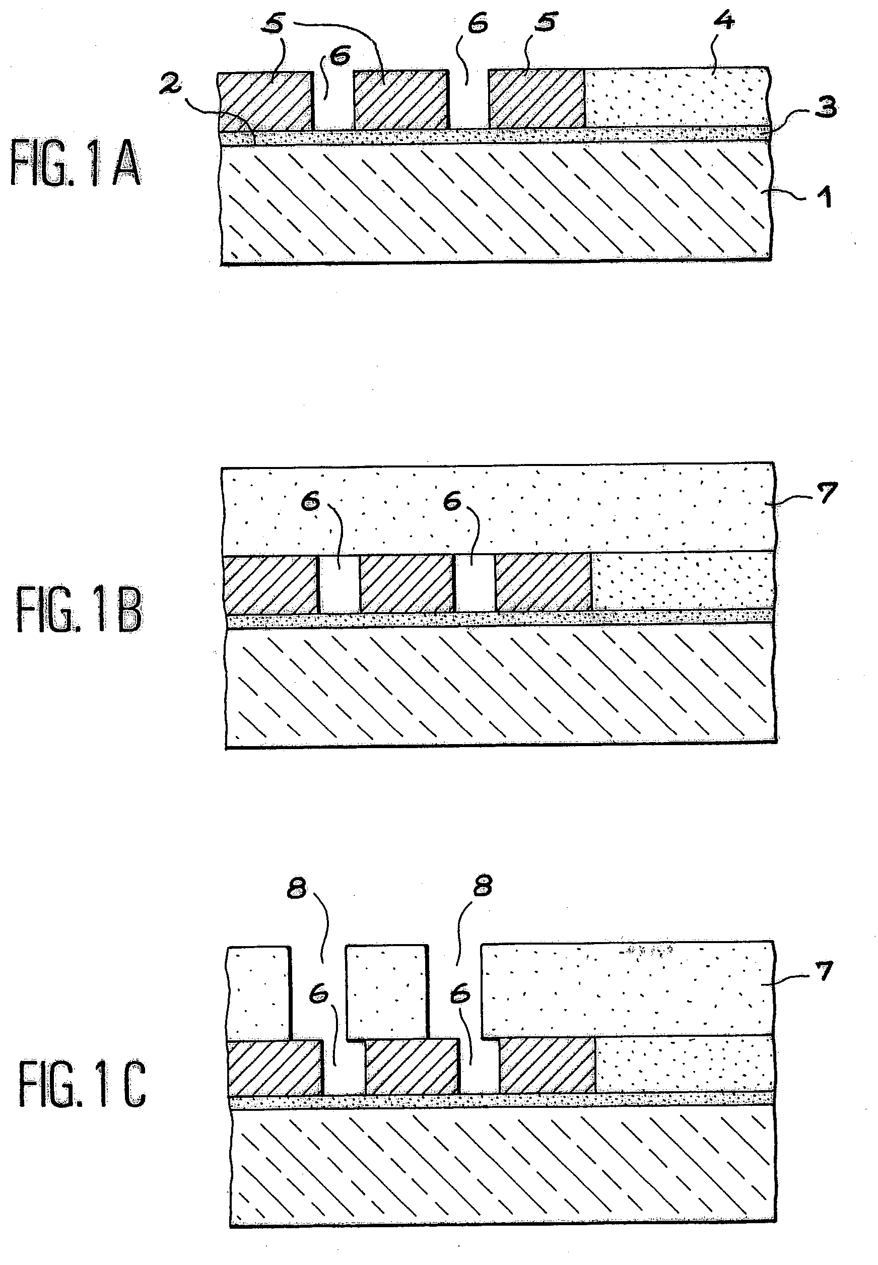
first embodiment
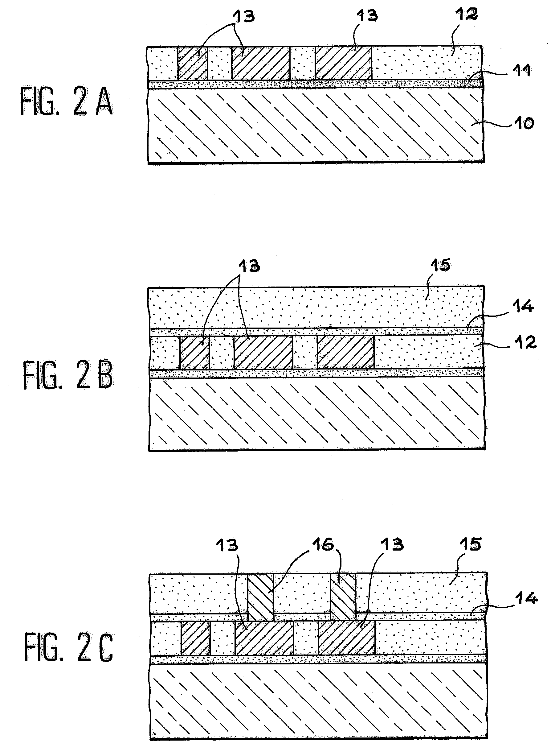
[0031] According to this first embodiment of the invention, the second electric insulating layer, 15, the interface layer 14 and the first electric insulating layer 12 are eliminated. Thus the structure shown in FIG. 2D is obtained.
[0032] A dielectric material 17 with low permittivity is deposited on this structure, a material known as a low-k (permittivity less than 3): for example, a polymer, SiOC, a porous dielectric material (for example, a material from the Nanoglass trademark), HSQ. The material 17 may be deposited by spreading or by chemical vapour deposition (CVD). It may involve, in this case, material with a high level of viscosity, a polymer with a long monomer chain. Some adapted deposit methods may also be used (PECVD, etc . . . ), which leave gaps in the small-sized spaces between the metals. FIG. 2E shows this step of the method and especially shows the presence of gaps 18 between the conducting lines 13. This Figure also shows that the conducting vias 16 are covered ...
second embodiment
[0034] FIGS. 3A to 3D illustrate the invention based on a silicon substrate.
[0035] The first steps of this second embodiment are identical to those illustrated in FIGS. 2A to 2C. Therefore they shall not be shown.
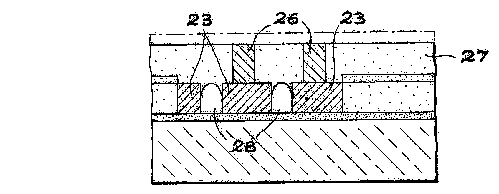
[0036] FIG. 3A shows the structure obtained after the elimination of the second electric insulating layer. As a variation, the interface layer located between the two layers of electric insulation could also be eliminated. The substrate 20 supports an interface layer 21, and the latter itself is covered by the first electric insulating layer 22 integrating the conducting lines 23. The interface layer 24 covers this first level of conductors, with the conducting vias 26 thereby ensuring the electric link with some conducting lines 23.
[0037] A layer of photosensitive resin is then deposited on the structure to form, by lithography, a mask 29 protecting the areas where the spaces between the lines 23 are large, for example, over 0.5 .mu.m (see FIG. 3B).
[0038] The areas in the ...
PUM
 Abstract
Description
Claims
Application Information