
Delay locked loop circuit and method having adjustable locking resolution

a technology of locking resolution and loop circuit, which is applied in the direction of digital storage, pulse technique, instruments, etc., can solve the problems of deteriorating high frequency operation of semiconductor integrated circuit, and affecting the stability of the circui

Inactive Publication Date: 2003-05-08
SAMSUNG ELECTRONICS CO LTD
View PDF0 Cites 38 Cited by
  • Summary
  • Abstract
  • Description
  • Claims
  • Application Information

AI Technical Summary

Problems solved by technology

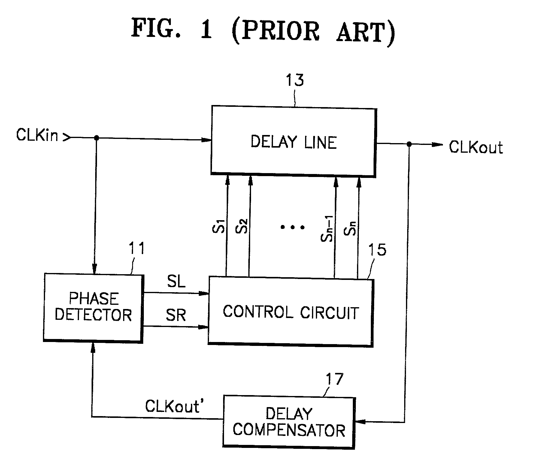
As such, as clock frequency increases, it becomes more and more difficult to maintain synchronization between the various component parts of the semiconductor integrated circuit.
Also, the delay of the clock signal can deteriorate the high frequency operation of the semiconductor integrated circuit.
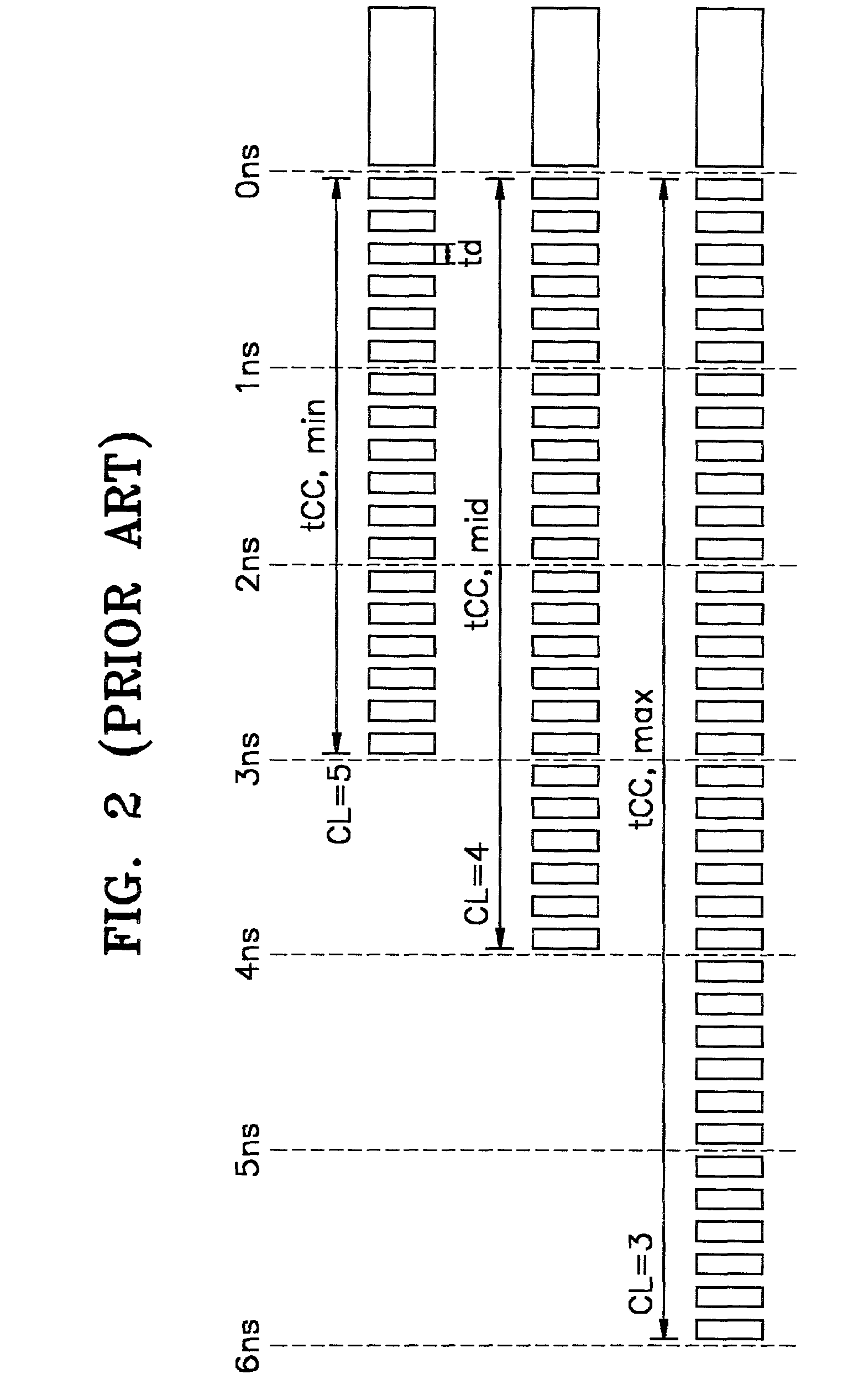
As such, the locking time becomes undesirably long.
On the other hand, the delay time of the unit delay circuits must be made relatively short when operating in the high-frequency domain to achieve the necessary locking resolution, and accordingly, the number of cycles of the worst case locking time in the low frequency domain is unavoidably increased.

Method used


Image

  • Delay locked loop circuit and method having adjustable locking resolution
  • Delay locked loop circuit and method having adjustable locking resolution
  • Delay locked loop circuit and method having adjustable locking resolution

Examples


first embodiment

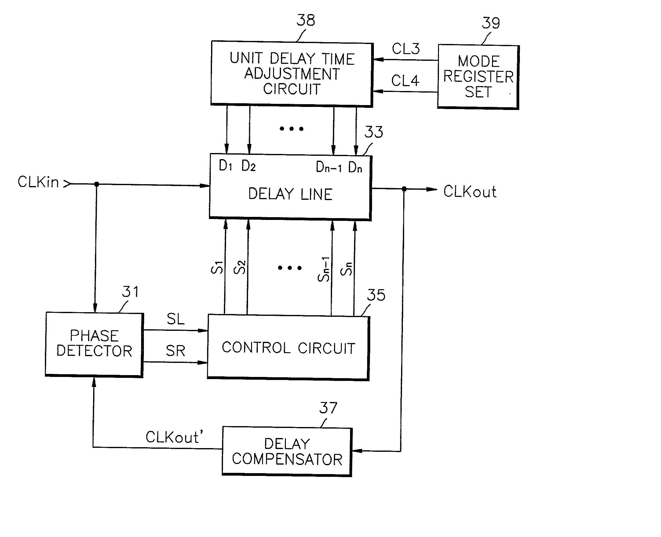
[0029] FIG. 3 is a block diagram of a DLL circuit according to the present invention. The DLL circuit of this embodiment includes a phase detector 31, a delay line 33, a control circuit 35, a delay compensator 37, a unit delay time adjustment circuit 38, and a Mode register set 39.

[0030] As shown, an external clock signal CLKin is delayed by the delay line 33 to produce an internal clock signal CLKout which is delayed relative to the external clock signal CLKin. The delay line 33 includes a plurality of unit delay circuits (not shown) which are selectively enabled in response to respective control signals S1 through Sn. The unit delay circuits are cascaded (connected in series) such that an amount of delay of the internal clock signal CLKout relative to the external clock signal CLKin depends on a number of the unit delay circuits which are effectively enabled by the control signals S1 through Sn.

[0031] The phase detector 31 receives a signal CLKout' (which is the internal signal CL...

second embodiment

[0054] FIG. 7 is a block diagram of a DLL circuit according to the present invention. The DLL circuit of this embodiment includes a phase detector 71, a delay line 73, a control circuit 75, a delay compensator 77, and a Mode register set 79.

[0055] As shown, an external clock signal CLKin is delayed by the delay line 73 to produce an internal clock signal CLKout which is delayed relative to the external clock signal CLKin. The delay line 73 includes a plurality of unit delay circuits (not shown) which are selectively made operational in response to respective control signals S1 through Sn. The unit delay circuits are cascaded (connected in series) such that an amount of delay of the internal clock signal CLKout relative to the external clock signal CLKin depends on a number of the unit delay circuits which are enabled by the control signals S1 through Sn.

[0056] The phase detector 71 receives a signal CLKout' (which is the internal signal CLKout after passing through the delay compens...


PUM


Abstract

A delay line receives an input clock signal and includes a cascaded plurality of unit delay circuits. A mode register set stores a value indicative of a column-address-strobe (CAS) latency of the memory device, and an adjustment circuit varies a delay time of the unit delay circuits according to the CAS latency stored in the mode register set. A phase detector detects a phase difference between the input clock signal and an output clock signal of the delay line, and a control circuit which controls an enabled state of the unit delay circuits according to an output of said phase detector.

Description

[0001] 1. Filed of the Invention[0002] The present invention generally relates to methods and circuits for delaying a reference clock signal to obtain a delayed clock signal which is delayed relative to the reference clock signal, and more particularly, the present invention relates to delay locked loop (DLL) circuits and methods.[0003] 2. Description of the Related Art[0004] A delay locked loop (DLL) circuit functions to delay a reference clock signal by a preset time period to thereby generate a delayed clock signal which is delayed relative to the reference clock signal. The generation of delayed clock signals is generally necessary in certain circuits which exhibit relatively high integration densities and which are synchronized with external clock signals. Such circuits include Rambus DRAMs (RDRAMs) and Synchronous DRAMs (SDRAMs).[0005] Generally, external clock signals are supplied via an input pin of a semiconductor integrated circuit, and from there they are distributed to v...

Claims


Application Information

Patent Timeline
IPC IPC(8): H03K5/135G11C7/10G11C7/22G11C8/00G11C11/407G11C11/4076H03L7/081H03L7/089
CPCG11C7/1045G11C7/22G11C7/222H03L7/0891H03L7/0814H03L7/089H03L7/0812H03L7/0816G11C8/00
Inventor HEO, NAK WONJUN, YOUNG HYUN
Owner SAMSUNG ELECTRONICS CO LTD
Learn More