Light emitting device and manufacturing method thereof

a technology of light-emitting devices and manufacturing methods, which is applied in the direction of organic semiconductor devices, identification means, instruments, etc., can solve the problems of reducing brightness, difficult to generate noise, and thus dark brightness

Inactive Publication Date: 2003-05-22
SEMICON ENERGY LAB CO LTD
View PDF2 Cites 54 Cited by
  • Summary
  • Abstract
  • Description
  • Claims
  • Application Information

AI Technical Summary

Problems solved by technology

Further, since the light emitting element is a carrier injection type light emitting element, it can be driven by a direct current voltage and a noise is hard to generate.
There is a problem, however, with this type of light emitting element in that charge accumulates in an organic compound layer when using direct current drive, in w...

Method used


Image

  • Light emitting device and manufacturing method thereof
  • Light emitting device and manufacturing method thereof
  • Light emitting device and manufacturing method thereof

Examples


embodiment 1

[0071] Embodiment 1

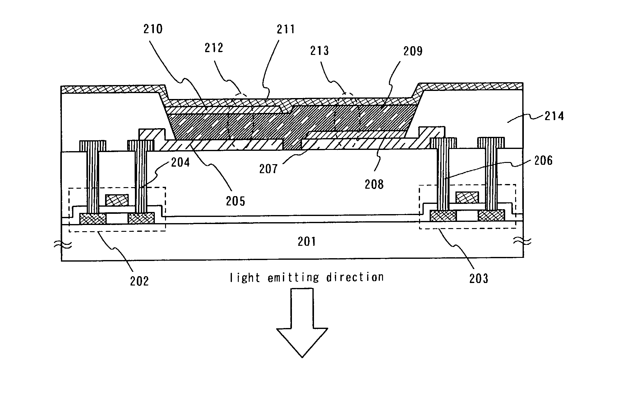
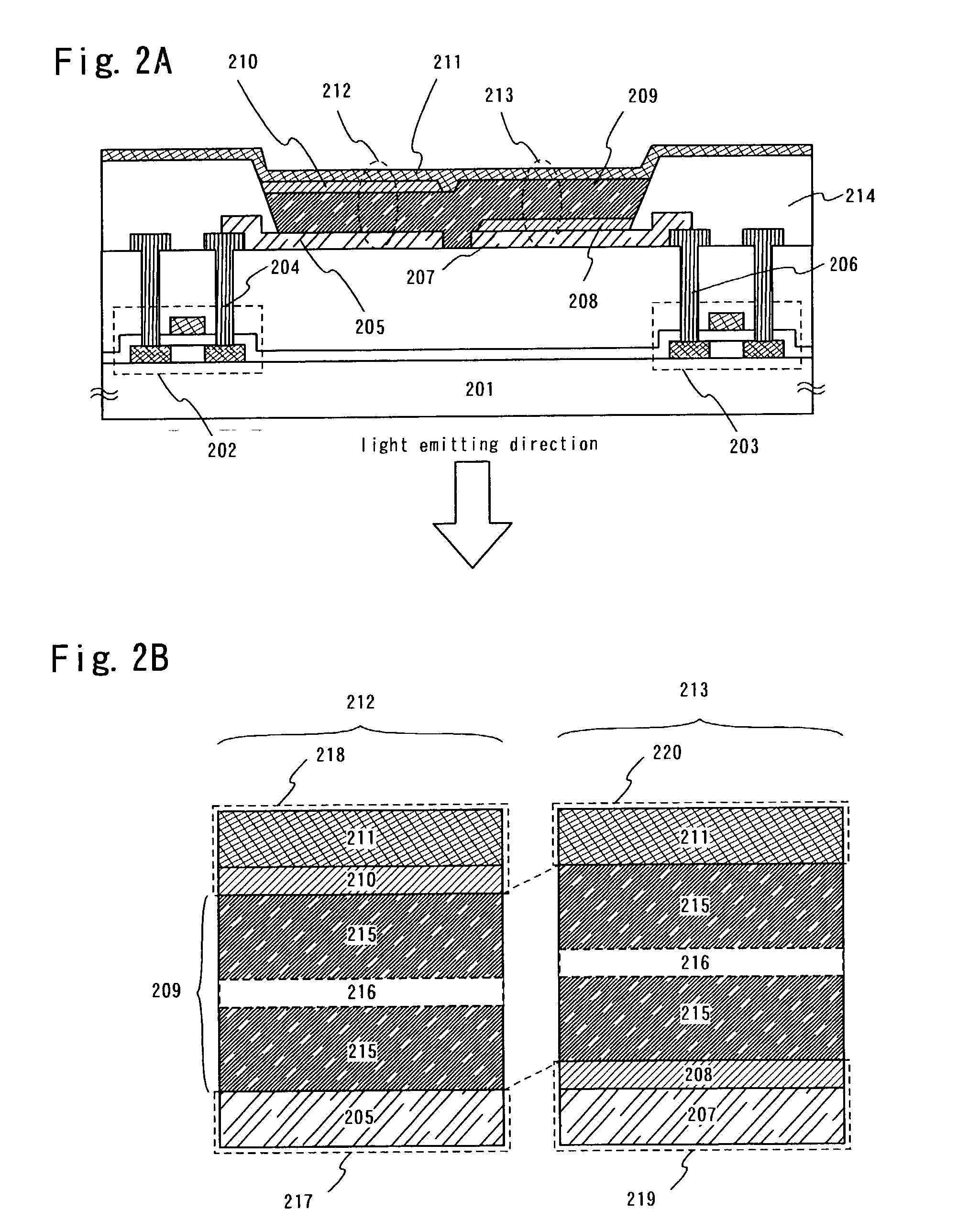
[0072] An active matrix structure in which TFTs (thin film transistors) and light emitting elements are electrically connected is explained in Embodiment 1. There is explained a case in which pixel electrodes of the light emitting elements are formed by transparent materials, and light developing in organic compound layers is extracted from the pixel electrodes (so-called bottom emission).

[0073] A cross sectional diagram of a pixel forming a pixel portion of a light emitting device is shown in FIG. 2A. Two types of TFTs (electric current control TFT) are formed on a substrate 201, a first electrode 205 is electrically connected to a TFT1 (202) through a wiring 204, and a second electrode (2) 207 is electrically connected through a wiring 206. Note that the TFT1 (202) is formed by a p-channel TFT in Embodiment 1, and the TFT2 (203) is formed by an n-channel TFT.

[0074] Note that the wiring 204 and a connection portion of the first electrode 205, and the wiring 206 a...

embodiment 2

[0096] Embodiment 2

[0097] A structure in which light developing in an organic compound layer is extracted from an opposing electrode (so-called top emission), and in which the opposing electrode is formed by a material having transparency, differently from Embodiment 1, is explained in Embodiment 2.

[0098] A cross sectional diagram of a pixel forming a pixel portion of a light emitting device is shown in FIG. 3A. Two types of TFTs (electric current control TFTs) are formed on a substrate 301, a first electrode 305 is electrically connected to a TFT1 (302) through a wiring 304, and a second electrode (2) 307 is electrically connected through a wiring 306. Note that the TFT1 (302) is formed by a p-channel TFT, and the TFT2 (303) is formed by an n-channel TFT in Embodiment 2.

[0099] Note that the wiring 304 and a connection portion of the first electrode 305, and the wiring 306 and a connection portion of the second electrode 307 are covered by an insulating layer 314 made from an insula...

embodiment 3

[0119] Embodiment 3

[0120] A case of a top emission light emitting device which is the same as the top emission light emitting device shown in Embodiment 2 and has an element structure different therefrom is explained in Embodiment 3.

[0121] A cross sectional diagram of a pixel forming a pixel portion of a light emitting device is shown in FIG. 4A. Two types of TFTs (electric current control TFTs) are formed on a substrate 401, a first electrode 405 is electrically connected to a TFT1 (402) through a wiring 404, and a second electrode (2) 407 is electrically connected through a wiring 406. Note that the TFT1 (402) is formed by an n-channel TFT, and the TFT2 (403) is formed by a p-channel TFT in Embodiment 1.

[0122] Note that the wiring 404 and a connection portion of the first electrode 405, and the wiring 406 and a connection portion of the second electrode 407 are covered by an insulating layer 414 made from an insulating material as in Embodiment 1. Note also that the insulating lay...


PUM


Abstract

A light emitting device is provided, which uses alternating current drive as a method of driving the light emitting device, and in which light emission is always obtained when voltages having different polarities are alternately applied, and a method of manufacturing the light emitting device is also provided. A first light emitting element made from an anode, an organic compound layer, and a cathode, and a second electrode made from an anode, an organic compound layer, and a cathode are formed. The light emitting elements are formed sandwiching the same organic compound layer. The anode of the first light emitting element and the anode of the second light emitting element, and the cathode of the first light emitting element and the cathode of the second light emitting element, are formed on opposite sides of the organic compound layer, respectively, thus sandwiching the organic compound layer. Note that voltages having an inverse polarity are applied alternately by the alternating current drive, and therefore light can always be emitted by any one of the first light emitting element or the second light emitting element.

Description

[0001] 1. Field of the Invention[0002] The present invention relates to a light emitting device and a manufacturing method thereof using a light emitting element which has a film containing an organic compound (hereinafter referred to as an "organic compound layer") between a pair of electrodes and which can give fluorescence or luminescence by receiving an electric field. The light emitting device referred to in the present specification is an image display device, a light emitting device or a light source. Additionally, the following are included in examples of the light emitting device: a module wherein a connector, for example, a flexible printed circuit (FPC) or a tape automated bonding (TAB) tape, or a tape carrier package (TCP)) is set up onto a light emitting element; a module wherein a printed wiring board is set to the tip of a TAB tape or a TCP; and a module wherein integrated circuits (IC) are directly mounted on a light emitting element in a chip on glass (COG) manner.[...

Claims


Application Information

Patent Timeline
IPC IPC(8): H05B33/26G09F9/00G09F9/30H01L27/32H01L51/50H01L51/52H05B33/00H05B33/10H05B33/12
CPCH01L27/3244H01L27/3281H01L51/5203H01L51/5206H01L2251/564H01L51/5221H01L51/5228H01L2251/5315H01L51/5212H10K59/12H10K59/17H10K50/80H10K50/81H10K50/814H10K50/824H10K2102/3026H10K71/841H10K59/805H05B33/00H10K50/805
Inventor YAMAZAKI, SHUNPEISEO, SATOSHI
Owner SEMICON ENERGY LAB CO LTD
Why Eureka
Try Eureka