
Selective address translation in coherent memory replication
a technology of coherent memory and address translation, applied in the field of address translation, can solve the problems of limited usefulness of multiprocessor computer systems, shared bus architectures, invalidated copies of previous data,
- Summary
- Abstract
- Description
- Claims
- Application Information
AI Technical Summary
Problems solved by technology
Method used
Image

Examples
Embodiment Construction
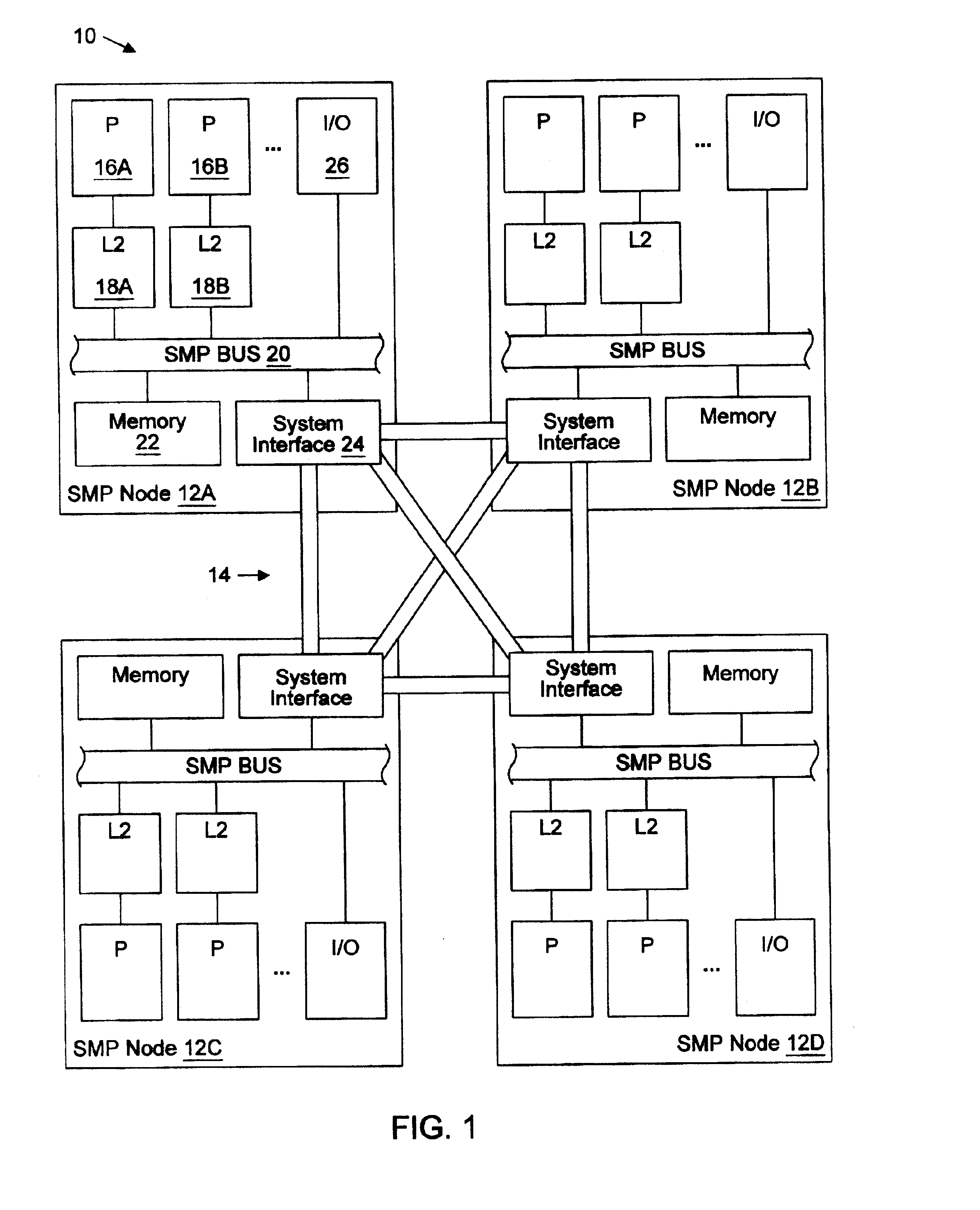
[0045] Turning now to FIG. 1, a block diagram of one embodiment of a multiprocessing computer system 10 is shown. Computer system 10 includes multiple SMP nodes 12A-12D interconnected by a point-to-point network 14. Elements referred to herein with a particular reference number followed by a letter will be collectively referred to by the reference number alone. For example, SMP nodes 12A-12D will be collectively referred to as SMP nodes 12. In the embodiment shown, each SMP node 12 includes multiple processors, external caches, an SMP bus, a memory, and a system interface. For example, SMP node 12A is configured with multiple processors including processors 16A-16B. The processors 16 are connected to external caches 18, which are further coupled to an SMP bus 20. Additionally, a memory 22 and a system interface 24 are coupled to SMP bus 20. Still further, one or more input / output (I / O) interfaces 26 may be coupled to SMP bus 20. I / O interfaces 26 are used to interface to peripheral ...
PUM
 Abstract
Description
Claims
Application Information