Chip self-test method and system

A chip self-test and self-test technology, applied in the direction of measuring electricity, measuring devices, measuring electrical variables, etc., can solve the problems of lost market opportunities, delayed product cycles, wasted test time and test resources, etc., to reduce test costs, ensure The effect of high accuracy and continuity

Active Publication Date: 2015-03-25
BYD SEMICON CO LTD
View PDF7 Cites 6 Cited by
  • Summary
  • Abstract
  • Description
  • Claims
  • Application Information

AI Technical Summary

Problems solved by technology

Once there is a problem with the realization of this function, the product design will return to the front-end stage, which greatly wastes testing time and testing resources, delays the product cycle, and may even lose market opportunities

Method used


Image

  • Chip self-test method and system
  • Chip self-test method and system
  • Chip self-test method and system

Examples


Embodiment Construction

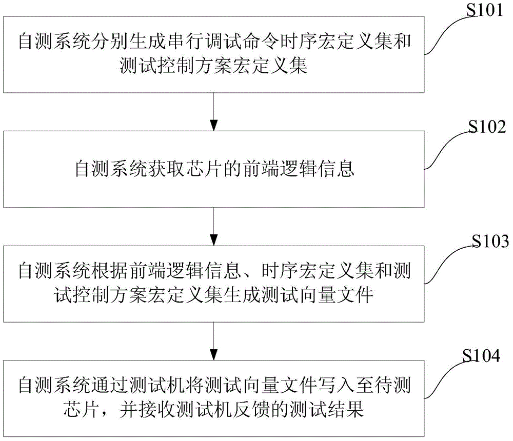
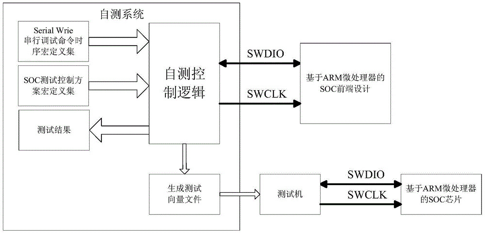
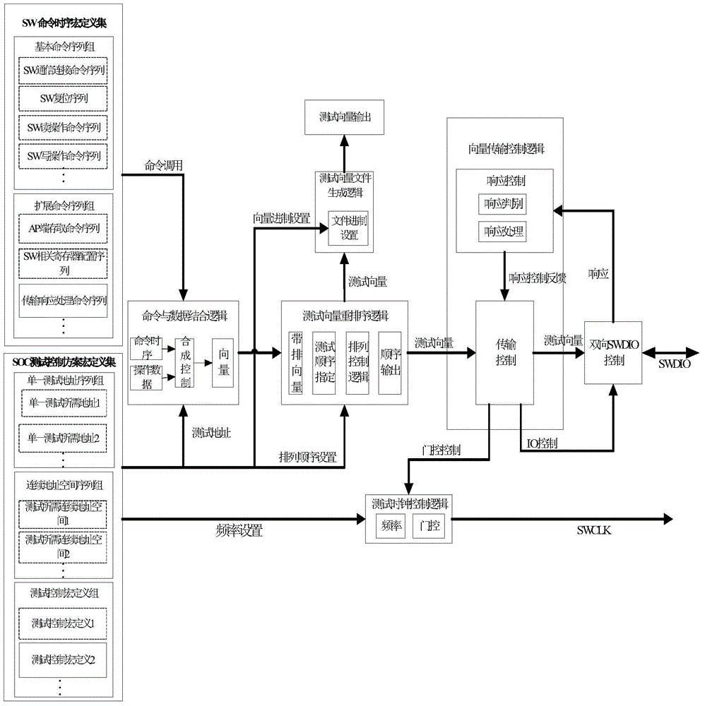
[0021] Embodiments of the present invention are described in detail below, examples of which are shown in the drawings, wherein the same or similar reference numerals designate the same or similar elements or elements having the same or similar functions throughout. The embodiments described below by referring to the figures are exemplary only for explaining the present invention and should not be construed as limiting the present invention.

[0022] In describing the present invention, it should be understood that the terms "center", "longitudinal", "transverse", "upper", "lower", "front", "rear", "left", "right", " The orientations or positional relationships indicated by "vertical", "horizontal", "top", "bottom", "inner" and "outer" are based on the orientations or positional relationships shown in the drawings, and are only for the convenience of describing the present invention and Simplified descriptions, rather than indicating or implying that the device or element refe...


PUM


Abstract

The invention provides a chip self-test method executed by a self-test system; the method comprises the following steps: the self-test system respectively generates a serial debug command sequential macrodefinition set and a test control scheme macrodefinition set; the self-test system obtains front end logic information of the chip; the self-test system generates a test vector file according to the front end logic information, the sequential macrodefinition set and the test control scheme macrodefinition set; the self-test system writes the test vector file into a tested chip through a test machine, and receives a test result returned by the test machine. The chip self-test method can fast and effectively verify SOC global address space, is simple in operation, easy to realize, and the method has high transplantability and connectivity; in addition, the method can save resources, and reduces test cost; the invention also provides the chip self-test system.

Description

technical field [0001] The invention relates to the field of embedded and SOC technologies, in particular to a chip self-test method and system. Background technique [0002] At present, in the field of embedded and SOC (System On Chip, system on a chip), in the design and verification stage, the internal triggers and functions of the SOC are generally tested and verified by loading external signal stimulus or downloading test software to drive the SOC. Implementation correctness, timing compliance, and system integrity. [0003] Specifically, in the front-end design verification stage, the debug interface function is not used, but the compiled test driver file is loaded into the SOC code storage model body through the EDA design simulation tool, and then the design is loaded with simulated external signal test stimulus, through the simulation The tool runs the test drive file and observes the test results for the purpose of testing and validating the design. In the engine...

Claims


Application Information

Patent Timeline
Patent Type & Authority Applications(China)
IPC IPC(8): G01R31/3177
Inventor 周博郭平日杨云
Owner BYD SEMICON CO LTD
Why Eureka
Try Eureka