
Depressed collector for electron beams

a collector and electron beam technology, applied in the field of electromagnetically active sources, can solve the problems of not being able to implement such devices for use with sheet electron beams, unable to meet the techniques of many devices including the submillimeter frequency backward wave oscillator, and unable to optimize circuitry efficiency of klystron without efficiency optimization circuitry

Inactive Publication Date: 2003-07-03
CALABAZAS CREEK RES
View PDF9 Cites 8 Cited by
  • Summary
  • Abstract
  • Description
  • Claims
  • Application Information

AI Technical Summary

Problems solved by technology

However, a klystron with no efficiency optimizing circuitry is typically only 40 to 50% efficient depending on the type of device used.
Despite the advantages of depressed collectors, no implementations of such devices have been reported for use with sheet electron beams, such as those which are utilized in submillimeter frequency Backward Wave Oscillators.
Consequently, most of the energy in the electron beam is deposited in the collector of the device where it must be dissipated as thermal power and typically requires cooling.
Unfortunately, many devices including the submillimeter frequency Backward Wave Oscillator are not amenable to the techniques utilized to implement depressed collectors in the prior art such as cylindrically symmetric vacuum tubes, traveling wave tubes and klystrons.
Simple depression of the existing collector geometry results in excessive generation of backscattered electrons and true secondary electrons.
The secondary electrons are accelerated at full voltage and impact on the main body of the device severely limiting the amount of energy that can be recovered from the electron beam.
An additional complication is the rectangular geometry of a device utilizing a rectangular sheet electron beam.
Finally, the Backward Wave Oscillator device operates at small currents (typically 30 to 40 milli-amperes) where space charge forces are small and techniques to control beam spread are limited by the presence of a strong, uniform magnetic field.
Nor is the device amenable to the use of induced variations in the magnetic field to achieve beam spread because the distance between the body of the device and the collector is inadequate in that the distance is less than 100 microns.
Variations of the magnetic field on this scale would be difficult to implement without adversely affecting beam transmission through the circuit.

Method used


Image

  • Depressed collector for electron beams
  • Depressed collector for electron beams
  • Depressed collector for electron beams

Examples


Embodiment Construction

[0016] The present invention provides a depressed collector capable of recovering energy from an electron beam emerging from the interaction region of a device producing electromagnetic wave radiation. The depressed collector incorporates an innovative electron trap and voltage depression to prevent the return of reflected electrons or true secondary electrons to the body or to the electron gun of the device.

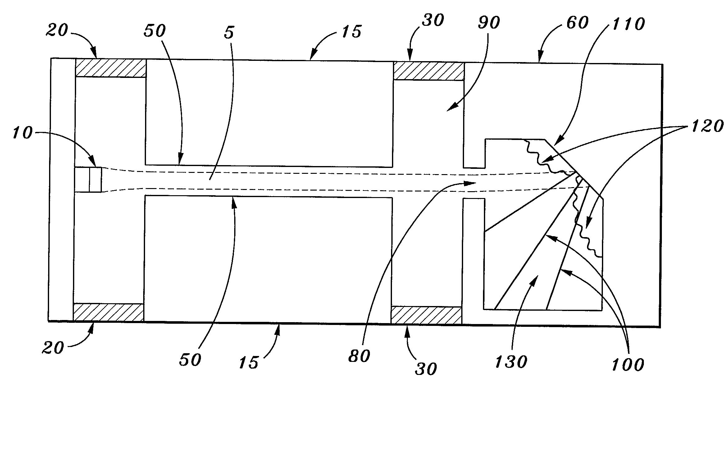
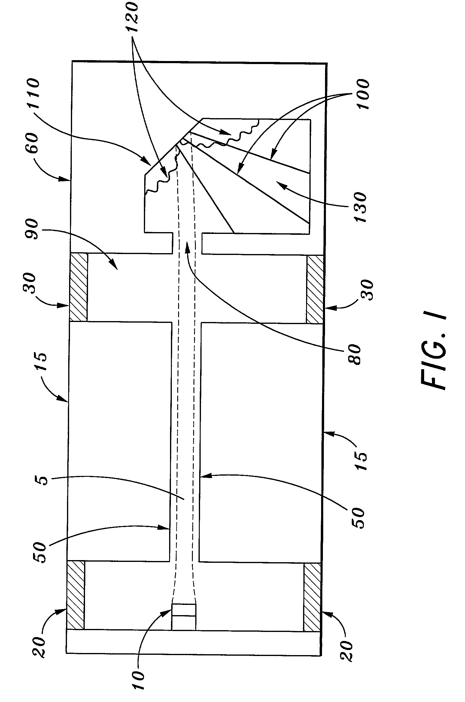
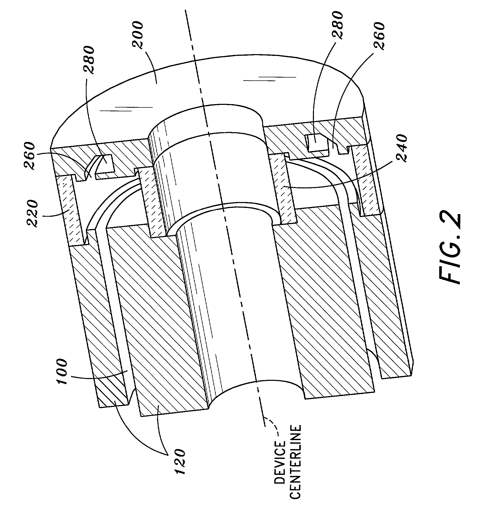
[0017] The operation of a single stage depressed collector in accordance with an embodiment of the invention in conjunction with a submillimeter frequency Backward Wave Oscillator is schematically illustrated in FIG. 1. A rectangular, sheet electron beam 5 is emitted from cathode 10 and passes through a rectangular beam tunnel 50 through the body 15 of the RF (radio frequency) device. Cathode 10 is energized to a voltage below that of the body sufficient to provide the required electron energy for interaction with the circuit of the device. The voltage potential between cathode ...


PUM


Abstract

A depressed collector for recovery of spent beam energy from electromagnetic sources emitting sheet or large aspect ration annular electron beams operating aver a broad range of beam voltages and currents. The collector incorporates a trap for capturing and preventing the return of reflected and secondary electrons.

Description

[0002] 1. Field of the Invention[0003] The present invention relates to electromagnetic wave sources utilizing rectangular sheet electron beams or annular electron beams, and more particularly, to an electron beam collector for such devices which allows for recovery of spent beam energy by the application of device geometry and voltage depression.[0004] 2. Background Art[0005] Linear beam electron devices are used in molecular spectroscopy, surveillance devices and sophisticated communications and radar systems that require generation or amplification of radio frequency or microwave electromagnetic signals. In UHF transmitters, the klystron is the most common power output device. However, a klystron with no efficiency optimizing circuitry is typically only 40 to 50% efficient depending on the type of device used. One scheme devised to improve klystron efficiency is the depressed collector, which allows for the recovery of energy from the electron stream rather than dissipating the e...

Claims


Application Information

Patent Timeline
IPC IPC(8): H01J23/02H01J23/027H03F3/56
CPCH01J23/027
Inventor IVES, R. LAWRENCE
Owner CALABAZAS CREEK RES
Learn More