

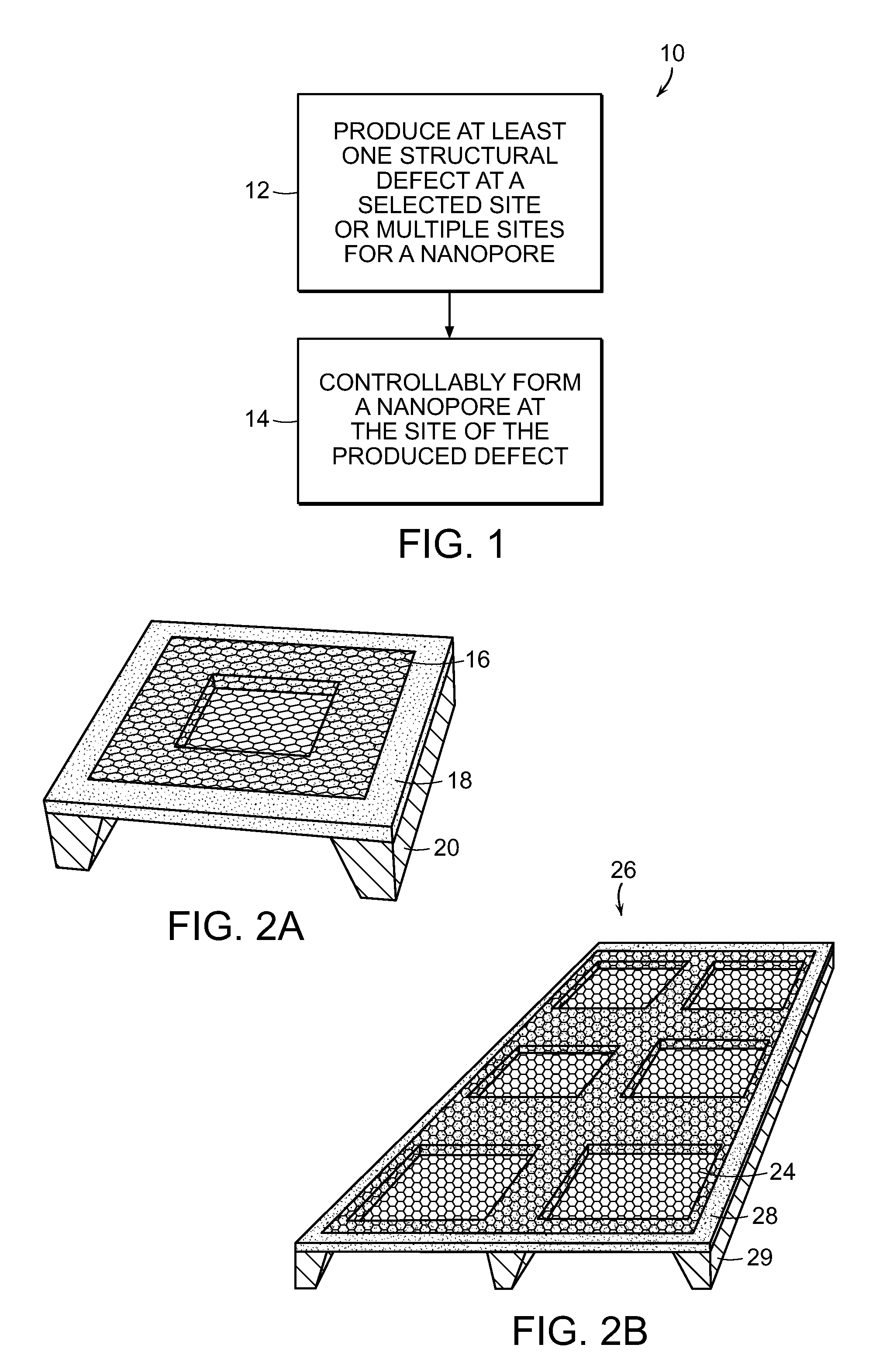
Controlled Fabrication of Nanopores in Nanometric Solid State Materials
a solid-state material and nano-scale technology, applied in the direction of instruments, synthetic resin layered products, vacuum evaporation coating, etc., can solve the problems of high-precision nanoscale processing that historically required a one-at-a-time fabrication paradigm, incompatible with nanoscale feature production and material manipulation, and high-volume batch fabrication techniques of conventional microelectronic production
- Summary
- Abstract
- Description
- Claims
- Application Information
AI Technical Summary
Benefits of technology
Problems solved by technology
Method used
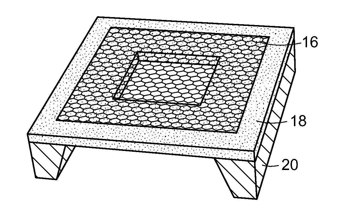
Image

Examples
example 1
Formation of a 20 Å Nanopore in Graphene
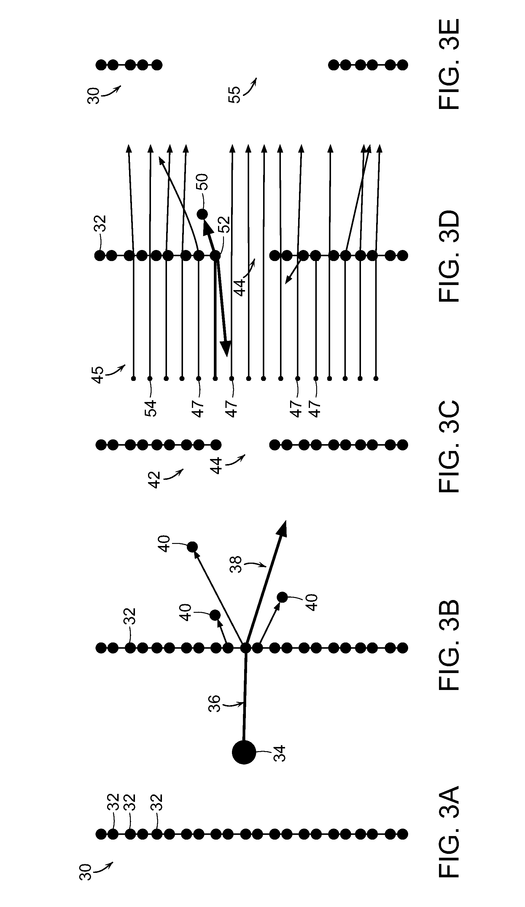
[0074]The nanometric material graphene was synthesized by chemical vapor deposition on a 25 μm-thick polycrystalline copper substrate (Aesar). The substrate was annealed at low pressure under continuous H2 flow at 1000° C. for ˜10 minutes, exposed to an additional flow of CH4 for ˜10 min at 1000° C. to grow the graphene, and then allowed to cool back to room temperature under continuous gas flow, requiring about 2 hours. After growth, the graphene was transferred to gold TEM grids covered in a thin amorphous carbon film with regular arrays of micron scale holes (Quantifoil, Au 1.2 / 2.0). A drop of deionized water was placed on the TEM grid and then the grid was placed on the graphene, which was pulled into contact with the graphene by the receding interface from the water droplet. The copper was then etched away from below by floating the structure on top of FeCl3 copper etchant (Transene). Once etched, the sample was then floated in 1N HCl to ...
example 2
Characterization of Graphene Nanopore Radius Correlation to Dose
[0081]To quantify the correlation between the radius of a nanopore in graphene as a function of dose of electrons employed to produce that nanopore radius, the two-step nanopore formation process of Example 1 was conducted, here with an ion beam dose of 1×10¹³ Ar+ / cm2 for producing nanopore nucleation sites in the graphene, and with an electron fluence of 3190±50 e− / Å2 / s for producing a nanopore at the sites. Sequential micrograph images containing multiple growing pores were obtained and analyzed by integrating the micrograph intensity over azimuthal angles as a function of radius, dividing by the circumference at that radius. The point of inflection of defocus at edge fringe was identified as the average radius of the nanopore.
[0082]Micrographs were drift corrected using a cross correlation algorithm and post-processed in ImageJ, with a low-pass filter to a 1.0 Å cutoff, adjusted to 8 bits of linear contrast about the...
example 3
High-Density Nanopore Formation in Graphene
[0085]Following the process of Example 1, a graphene region of 6.27×10⁵ Å2 was exposed first to a 3 keV beam of argon ions to impose a dose of 1×10¹³ Ar+ / cm2 in the formation of nanopore nucleation sites, and then exposed to an electron beam to impose a dose of 9.7×10⁶ e− / Å2 to form nanopores at the nucleation sites. FIG. 7 is a micrograph of the resulting structure, identifying 32 nanopores, as indicated by arrowheads. The locations of some of the smaller and larger nanopores in the image were determined by looking at preceding and subsequent images in a series of images. The resulting nanopore density corresponds to 5.1×10¹¹ nanopores / cm2. This correlates with the ion beam dose of 1×10¹³ Ar+ / cm2 as each 3 keV Ar+ having a probability of about 5% of nucleating a nanopore under these irradiation conditions.
[0086]FIG. 8 is a plot of nanopore radius distribution for the nanopores shown in the image of FIG. 7. The nanopore radius distribution ...
PUM
| Property | Measurement | Unit |
|---|---|---|
| Temperature | aaaaa | aaaaa |
| Temperature | aaaaa | aaaaa |
| Fraction | aaaaa | aaaaa |
Abstract
Description
Claims
Application Information