Supercharge Your Innovation With Domain-Expert AI Agents!

Organic EL panel and method for manufacturing the same

a technology of organic el and el panels, which is applied in the direction of liquid surface applicators, coatings, semiconductor devices, etc., can solve the problems of insufficient separation, unstable size of overhanging portions 310, and difficulty in extending the service life of panels

Inactive Publication Date: 2003-07-03
SAMSUNG DISPLAY CO LTD
View PDF4 Cites 8 Cited by
  • Summary
  • Abstract
  • Description
  • Claims
  • Application Information

AI Technical Summary

Problems solved by technology

The generation of a dark spot makes it difficult to extend the service life of a panel.
Thus, the sizes of overhanging portions 310 are unstable and insufficient separations tend to occur.
When an insufficient separation occurs, not only are a cathode electrode 33 and an anode, transparent electrode 2 short-circuited and a non-emission element generated, but also the panel may be damaged by heat due to the short circuit.
As a result, the aperture ratio can not be increased, and it is difficult to attain a smaller pixel size.
However, if the partitions are too low, the incident angle is small, the film thickness is uneven and the color edges are not sharply defined.
If the partition is too high, however, control of the evaporation stream is difficult.
When the width of a partition 11 is narrower than 10 .mu.m, the emission layer 12 is not sufficiently separated, and the image quality may be deteriorated.
When the width of the partition 11 is wider than 40 .mu.m, however, the aperture ratio is reduced, and it is difficult to provide a smaller feature size for a pixel.

Method used


Image

  • Organic EL panel and method for manufacturing the same
  • Organic EL panel and method for manufacturing the same
  • Organic EL panel and method for manufacturing the same

Examples


Embodiment Construction

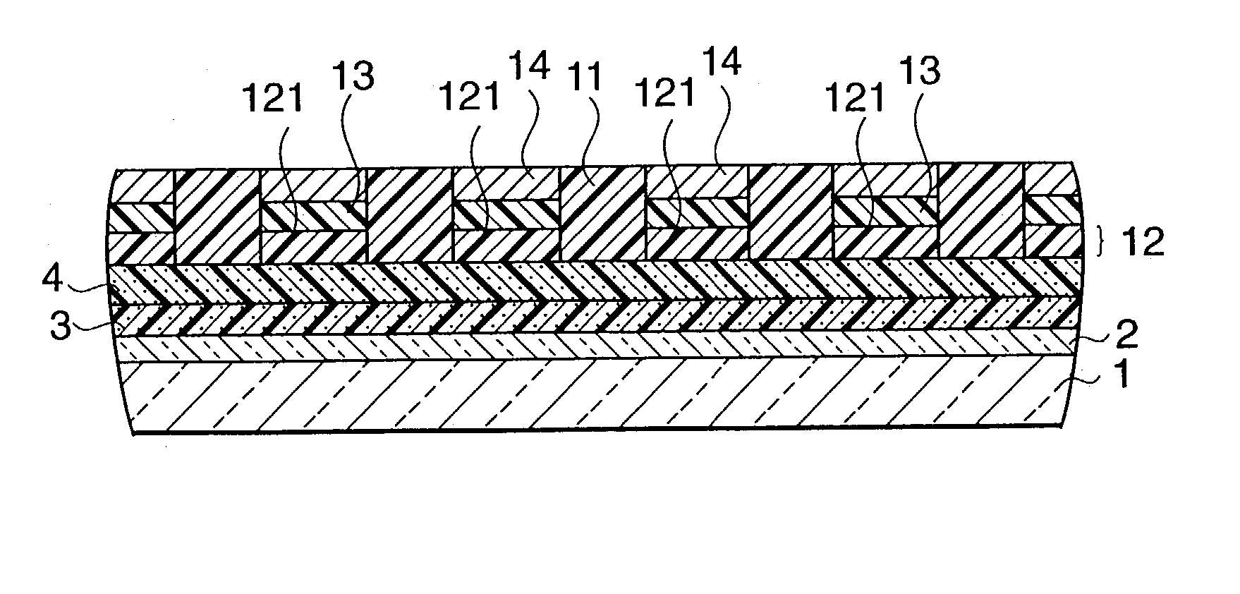
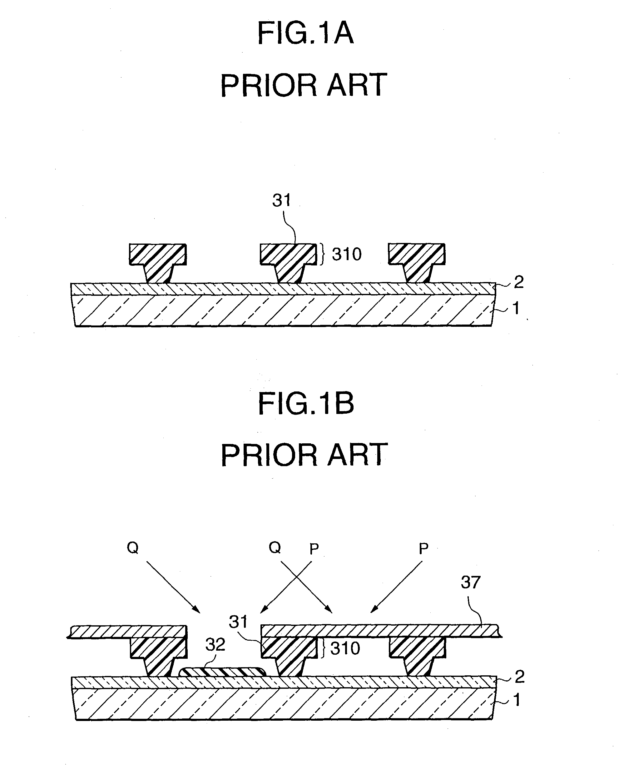
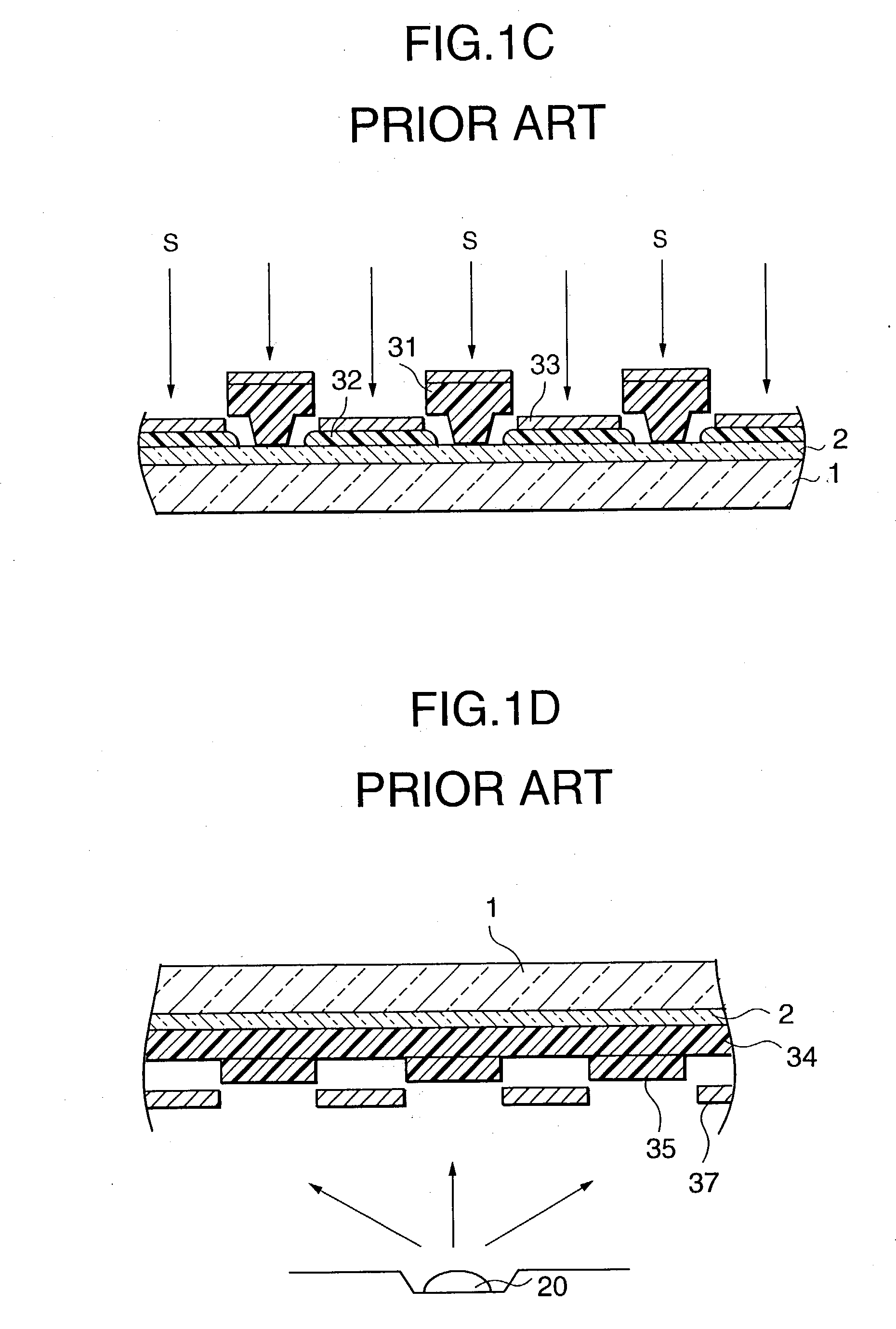
[0080] A conventional organic EL panel was manufactured, as shown in FIG. 1D, to use as a comparison with the above embodiments. An ITO thin film of 120 nm was deposited on a glass substrate 1 of 1.1 mm by sputtering, and transparent electrodes 2, which were anodes, were formed as stripes. The sheet resistance of the transparent electrodes 2 was 15 .OMEGA. / cm.sup.2, the wiring width was 250 nm, and the space was 20 .mu.m. Then, as a hole injection and transport layer, a 50 nm layer 34 of N,N'-diphenyl-N,N'-bis(.alpha.-naphthyl)-1,1'biphenyl-4,4'-diamine of was formed on the glass substrate 1 by using vacuum deposition. Next, a shadow mask 37 was positioned on the organic layer 34, perpendicular to the transparent electrode pattern, so that mask holes were aligned with the red color areas. As a red emission material, 4-dicyanomethylene-2-met-hyl-6-(p-dimethylaminostyryl)-4H-pyrane of 3 wt % was doped into tris(8-hydroxyquinolinol)aluminum, and this material was deposited on the organ...


PUM


Abstract

For an organic EL panel, whereon partitions are used to separate pixels, transparent electrodes, a charge generation layer and a charge transfer layer are formed in the named order on a substrate. Then, when the charge transfer layer is electrified and the charge generation layer is selectively exposed, an electrostatic latent image having a predetermined pattern is formed on the charge transfer layer. Subsequently, to form the partitions, the electrostatic latent image is developed by using a developing agent and the developing agent is fixed. Following this, emission layers and opposing electrodes to the transparent electrodes are positioned between the thus obtained partitions.

Description

[0001] 1. Field of the Invention[0002] The present invention relates to an organic electroluminescence (hereinafter referred to as EL) panel and a method of manufacturing the same, and more particularly to an organic EL panel provided with partitions for separating pixels and to a method of manufacturing the partitions.[0003] 2. Related Arts[0004] An organic EL panel having such partitions is disclosed in Japanese Unexamined Patent Publications No. Hei 9-102393 and Hei 8-315981. According to the organic EL panel manufacturing method disclosed in these publications, as is shown in FIG. 1A, anodes, transparent electrodes 2 composed of indium tin oxide (hereinafter referred to as ITO), are formed as stripes on a transparent substrate 1, and to separate the pixels, photolithography is used to form electrical insulating partitions 31 that cross and that are perpendicular relative to the transparent electrodes 2. The lower portions of these partitions 31 are tapered invertedly, and their ...

Claims


Application Information

Patent Timeline
Patent Type & Authority Applications(United States)
IPC IPC(8): H10K99/00
CPCH01L27/3211H01L27/3283H01L51/0004H01L51/0008H01L51/56H01L51/005H01L51/0059H01L51/0081H01L51/0017H10K59/353H10K59/173H10K71/13H10K71/16H10K71/231H10K85/60H10K85/631H10K85/324H10K71/40H10K71/12H10K71/164H10K71/00
Inventor SAKAGUCHI, YOSHIKAZU
Owner SAMSUNG DISPLAY CO LTD
Features
  • R&D
  • Intellectual Property
  • Life Sciences
  • Materials
  • Tech Scout
  • Unparalleled Data Quality
  • Higher Quality Content
  • 60% Fewer Hallucinations
Learn More