Bump fabrication process

a technology of fabrication process and bump, which is applied in the direction of manufacturing tools, basic electric elements, solid-state devices, etc., can solve the problems of increasing the production cost of bumps, and achieve the effect of saving one mask process

Inactive Publication Date: 2003-07-03
ADVANCED SEMICON ENG INC
View PDF0 Cites 30 Cited by
  • Summary
  • Abstract
  • Description
  • Claims
  • Application Information

AI Technical Summary

Benefits of technology

0014] The present invention provides a bump fabrication process by using the lift-off technology for lifting off the conductive layer on the

Problems solved by technology

Thus, one extra mask process can greatly i

Method used


Image

  • Bump fabrication process
  • Bump fabrication process
  • Bump fabrication process

Examples


Embodiment Construction

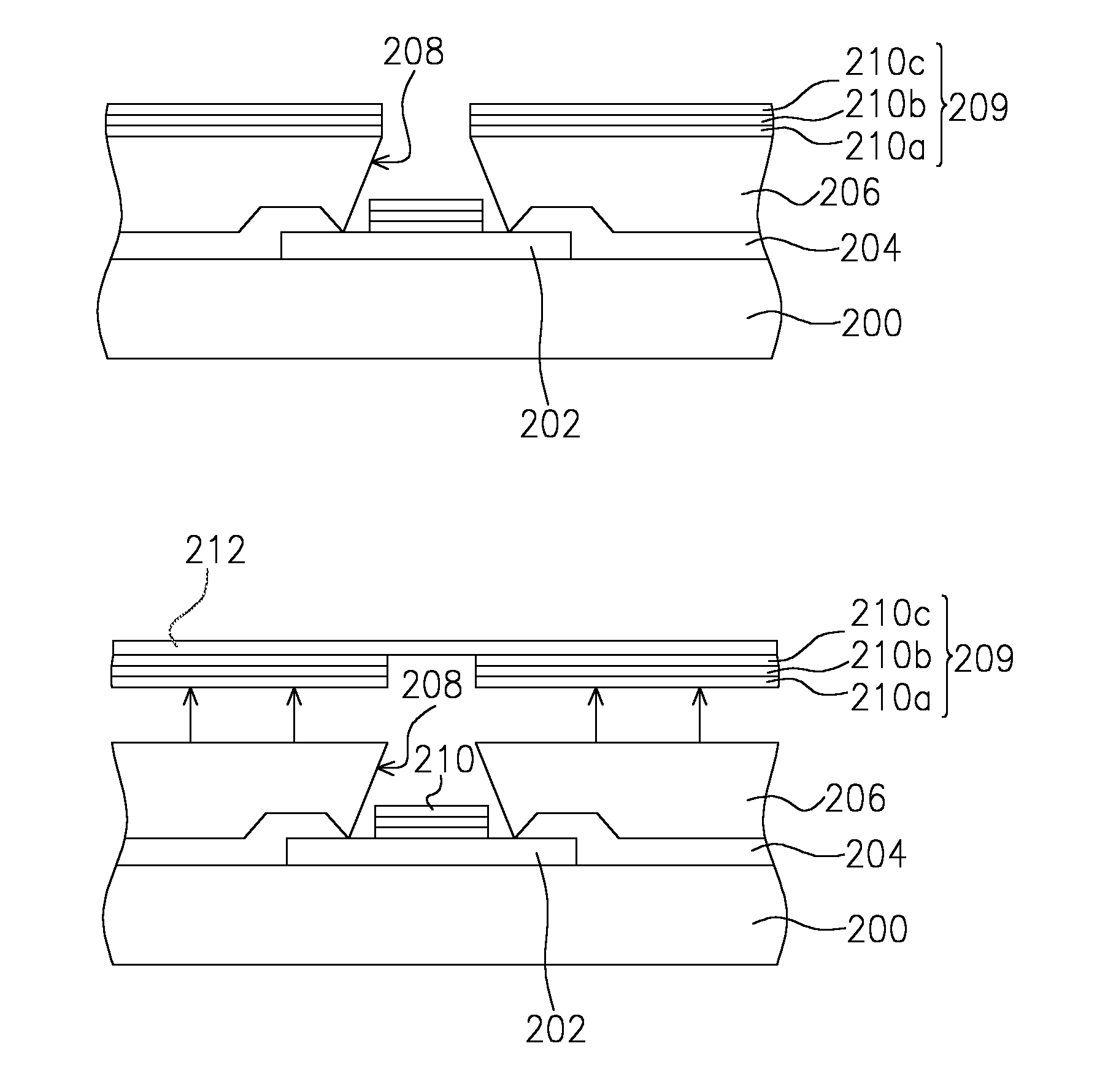
[0023] Figs. 8-14 are cross-sectional views illustrating steps of a bump fabrication process according to one preferred embodiment of this invention.

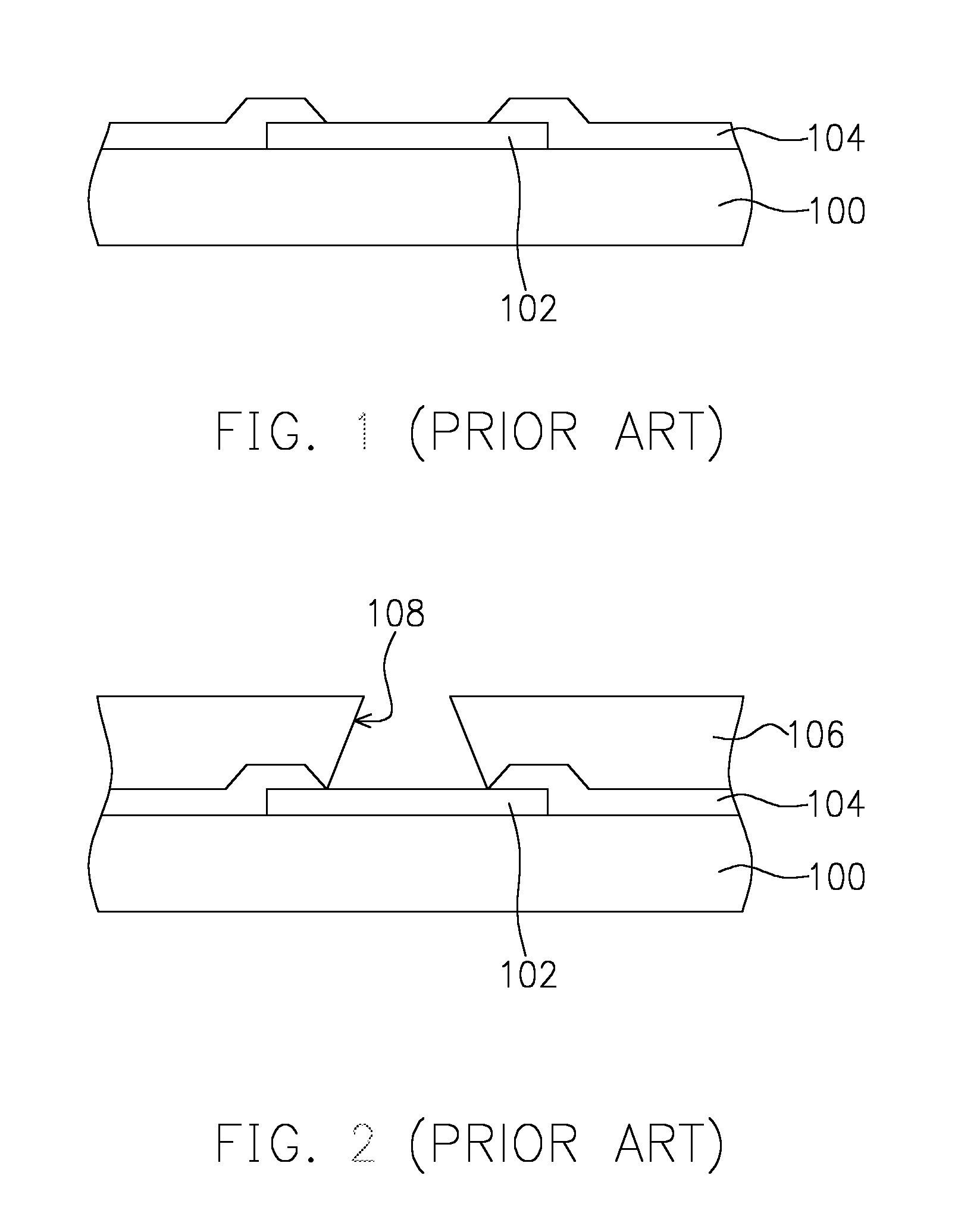
[0024] Referring to the Fig. 8, a substrate or wafer 200 is provided with a bonding pad 202 and a protective (passivation) layer 204. The protective layer 204 is disposed on the wafer 200, protecting a surface of the wafer 200 and exposing a surface of the bonding pad 202. The bonding pad 202 can be an aluminum pad or a copper pad, for example.

[0025] As shown in Fig. 9, a photoresist layer 206 having an opening 208 is formed over the wafer 200. The location of the opening 208 corresponds to the location of the bonding pad 202, so as to expose the surface of the bonding pad 202. The opening 208 has a structure similar to an undercut (an undercut structure), for example.

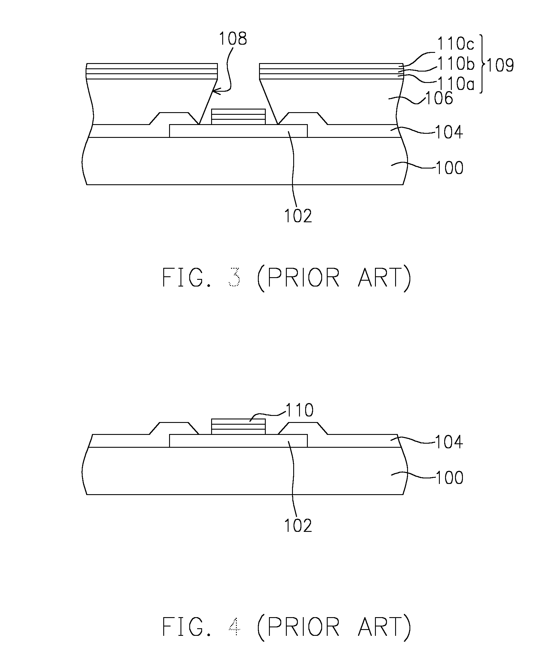
[0026] Referring to Fig. 10, a conductive layer 209 is formed over the wafer 200 and on the photoresist layer 206. The conductive layer 209 includes an adhesion layer 210a...


PUM

PropertyMeasurementUnit
Adhesion strengthaaaaaaaaaa
Electrical conductoraaaaaaaaaa
Adhesivityaaaaaaaaaa

Abstract

Abstract of Disclosure The present invention provides a bump fabrication process. A wafer is provided with a patterned photoresist layer formed on the wafer. The patterned photoresist layer has a plurality of openings, corresponding to bonding pads. A conductive layer is formed on the photoresist layer and the exposed bonding pads. Afterwards, a sticker film is provided to lift off the conductive layer on the photoresist layer, while the conductive layer within the openings is not removed. A solder paste is filled into the openings. A reflow step is performed to turn the filled solder paste into globular bumps. At last, the photoresist layer is removed.

Description

Cross Reference to Related Applications[0001] This application claims the priority benefit of Taiwan application serial no. 90133197, filed December 31, 2001.Background of Invention[0002] Field of Invention[0003] The present invention relates to a fabrication process for forming bumps. More particularly, the present invention relates to the lift-off technology for forming the under bump metallurgy layer in the bump fabrication process.[0004] Description of Related Art[0005] At present, the market of multimedia applications rapidly expands. The integrated circuit (IC) packaging needs to be improved following the developing trends of electronic devices such as digitalization, network localization, and user friendliness. In order to meet the above requirements, electronic devices must have multiple functions and high integration, and maintain high operating speed, miniaturization, lightweight, and low cost. High-density packages, such as ball grid arrays (BGAs), chip scale packages (CS...

Claims


Application Information

Patent Timeline
IPC IPC(8): H01L21/60H01L23/485
CPCH01L24/02H01L24/03H01L2924/00014H01L2224/1131H01L2924/01033H01L2924/01024H01L2924/01023H01L24/05H01L24/11H01L24/12H01L2224/0347H01L2224/0401H01L2224/05599H01L2224/11472H01L2224/11901H01L2224/13023H01L2224/131H01L2924/01006H01L2924/01013H01L2924/01022H01L2924/01029H01L2924/01074H01L2924/014H01L2924/14H01L2924/00013H01L2924/01005H01L2224/13099
Inventor TONG , HO-MINGLEE , CHUN-CHIFANG , JEN-KUANGHUANG , MIN-LUNGCHEN , JAU-SHOUNGSU , CHING-HUEIWENG , CHAO-FULEE , YUNG-CHICHOU , YU-CHEN
Owner ADVANCED SEMICON ENG INC
Why Eureka
Try Eureka