

X-ray detector and fabrication method thereof
- Summary
- Abstract
- Description
- Claims
- Application Information
AI Technical Summary
Benefits of technology
Problems solved by technology
Method used
Image

Examples
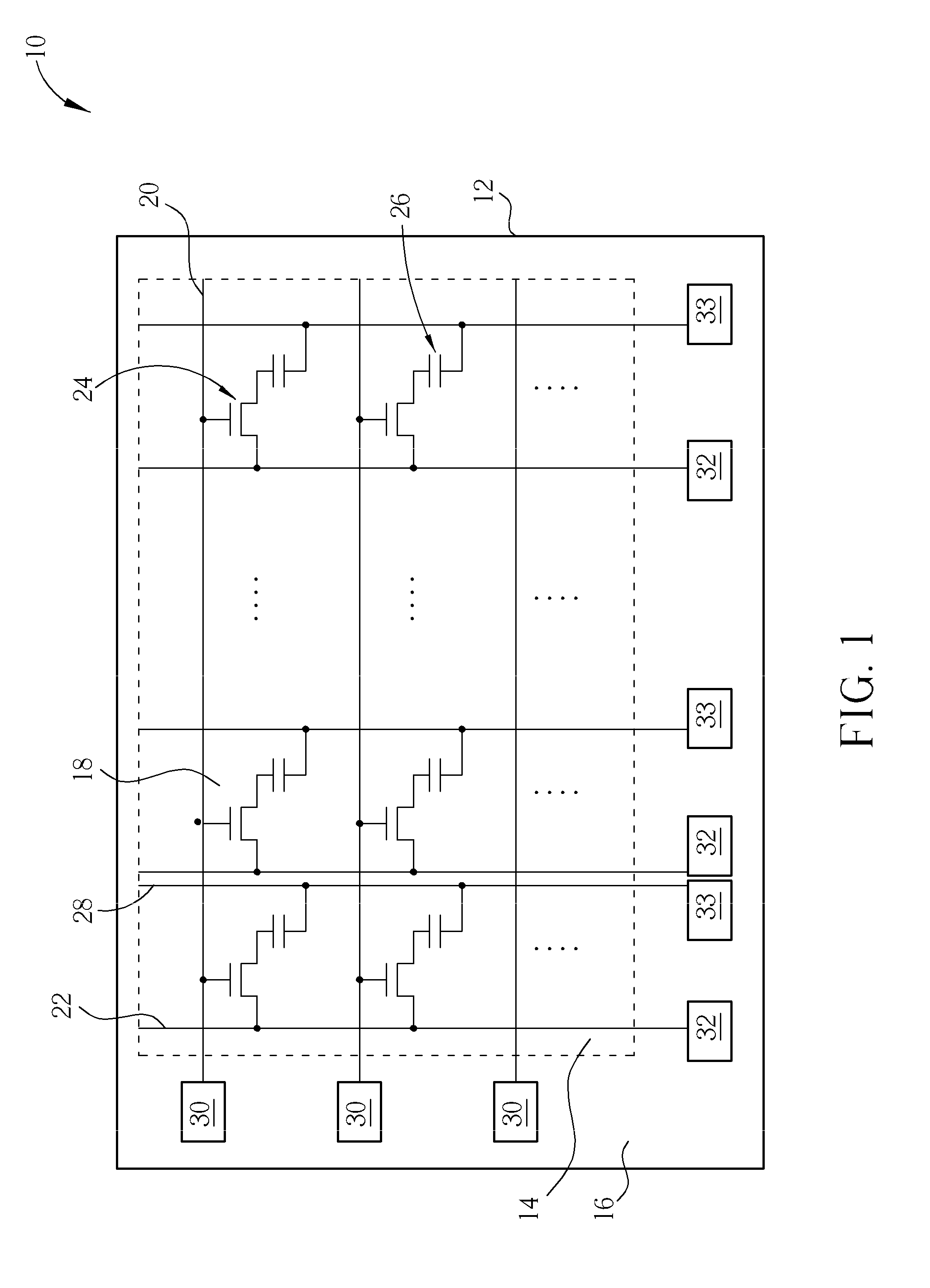
first embodiment
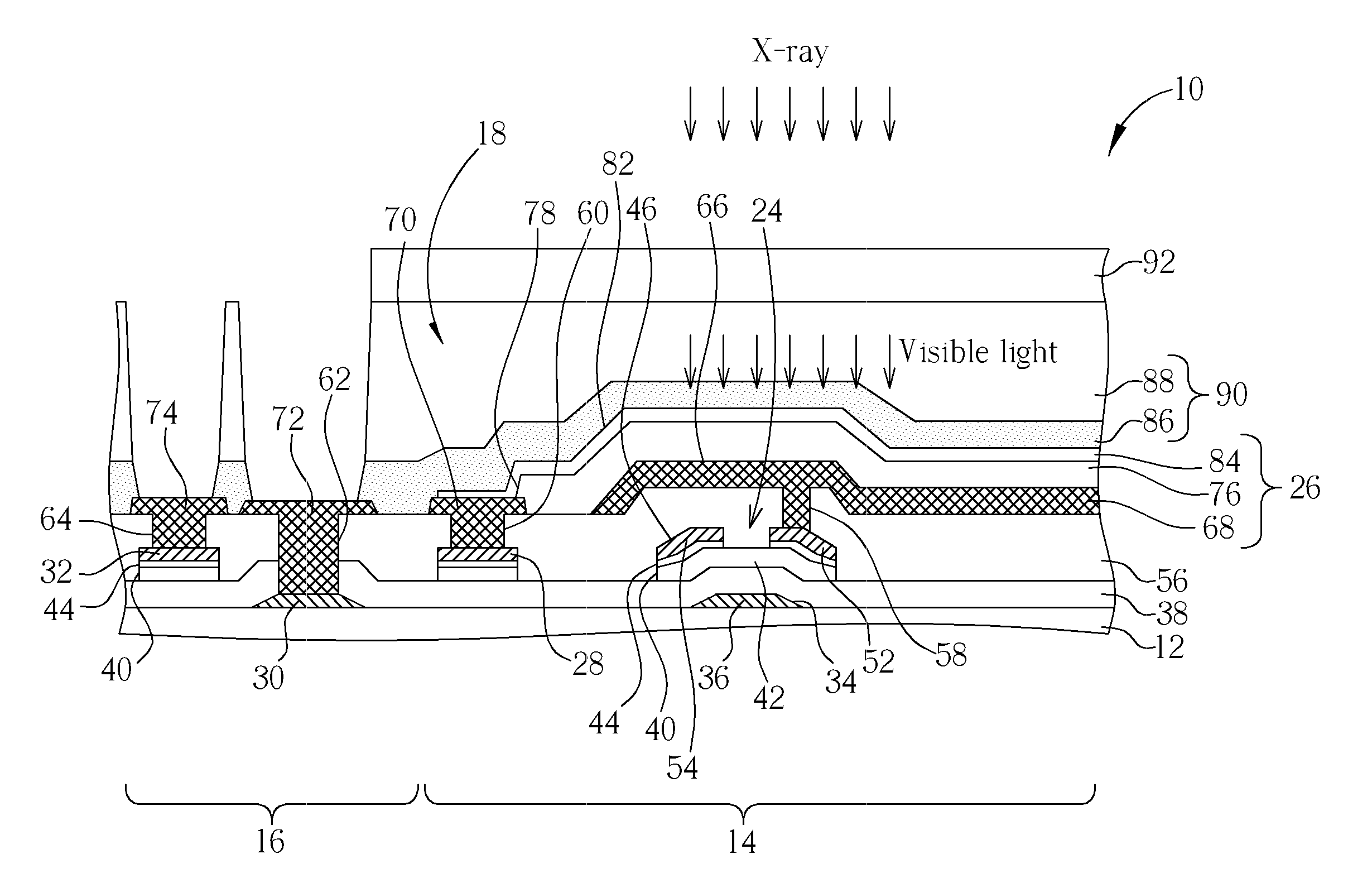
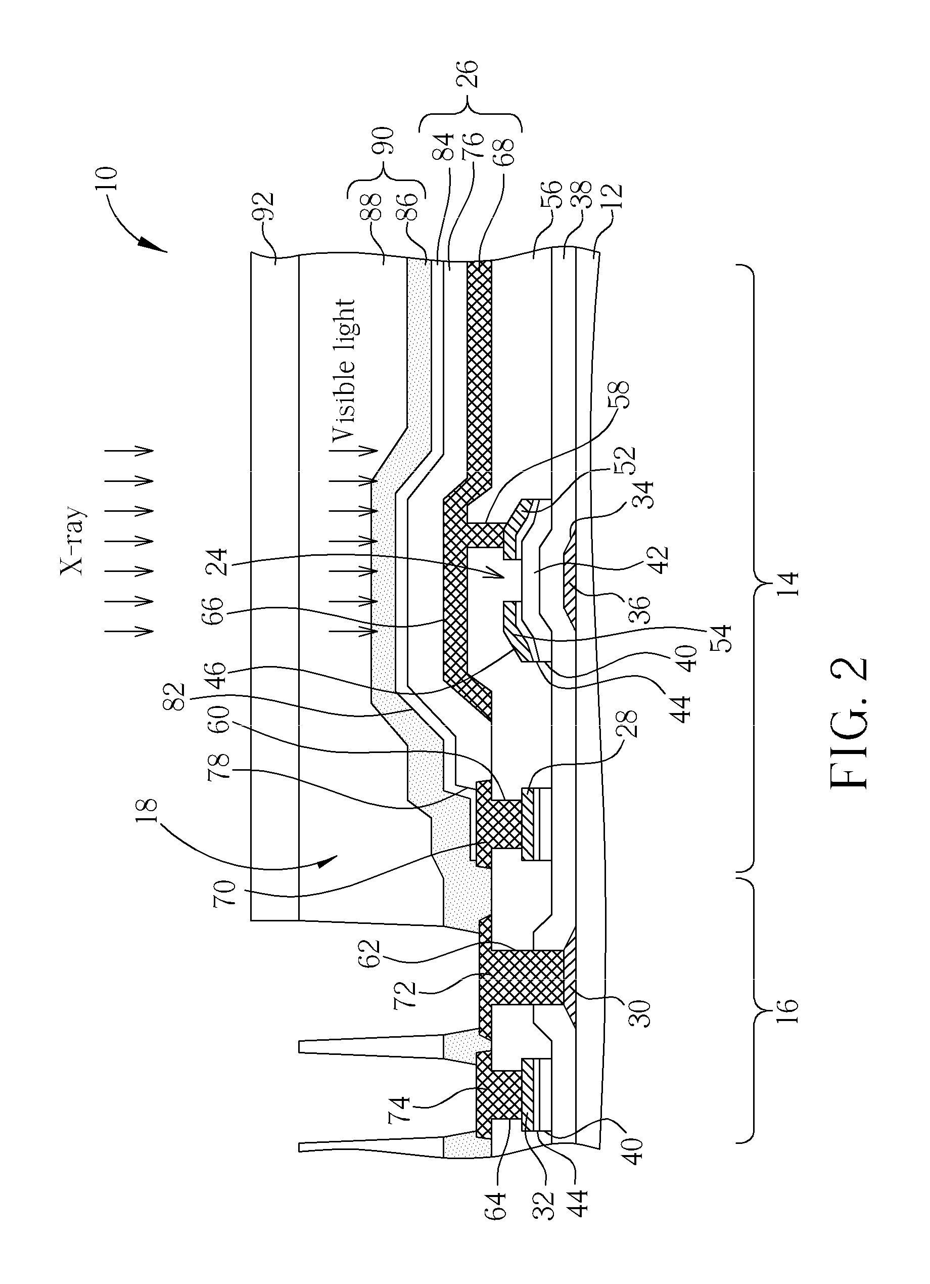
[0026]Sequentially, a passivation layer 90 is formed on the substrate 12, which comprises an inorganic passivation layer 86 and an organic planarization layer 88 covering the photo-sensing area 14 but exposing the first contact plug 72 and the second contact plug 74. Referring to FIG. 2, a scintillator layer 92 is then formed on the organic planarization layer 86 to cover the photo-sensing area 14. The formation step of the scintillator layer 92 may include a coating process or an evaporation process. In other embodiment, the scintillator layer 92 may be formed through an attaching process. After the formation of the scintillator layer 92, the fabrication of the X-ray detector 10 according to the present invention is completed. As a result, the whole fabrication process of the X-ray detector 10 only needs seven photolithography-etching processes.
[0027]With reference to FIG. 9 to FIG. 12, the fabrication process of the X-ray detector according to a second embodiment of the present in...
third embodiment
[0030]With reference to FIG. 13, FIG. 13 is a schematic diagram of an X-ray detector 100 according to the present invention. In this embodiment, the TFT of the X-ray detector 100 is formed through three photolithography-etching processes, and the scintillator layer 92 is directly formed on the surface of the passivation layer 90. It should be noted that the patterned transparent conductive layer 82 further covers the surfaces of the first and the second contact plugs 72, 74. The patterned transparent conductive layer 82 preferably comprises indium tin oxide (ITO) materials. Since ITO has high stability, the patterned transparent conductive layer 82 may provide a function to protect the first and second contact plugs 72, 74.
[0031]In addition, in other embodiments, the patterned second conductive layer 46 may do not include the top electrode line 28 shown in FIG. 13. In contrary, a portion of the patterned third conductive layer 66 is utilized to serve as the top electrode line and to...
PUM
 Abstract
Description
Claims
Application Information