LSI design verification apparatus, LSI design verification method, and LSI design verification program

a design verification and design technology, applied in computer aided design, electronic circuit testing, instruments, etc., can solve problems such as difficult sample of future signal values

Inactive Publication Date: 2003-07-03
KK TOSHIBA
View PDF12 Cites 34 Cited by
  • Summary
  • Abstract
  • Description
  • Claims
  • Application Information

AI Technical Summary

Problems solved by technology

With in the test bench description, a signal value of DUT of the past is possible to be sampled, but a signal value of the future is difficult to be sampled.

Method used


Image

  • LSI design verification apparatus, LSI design verification method, and LSI design verification program
  • LSI design verification apparatus, LSI design verification method, and LSI design verification program
  • LSI design verification apparatus, LSI design verification method, and LSI design verification program

Examples


first embodiment

[0075] Architecture of LSI Design Verification Apparatus

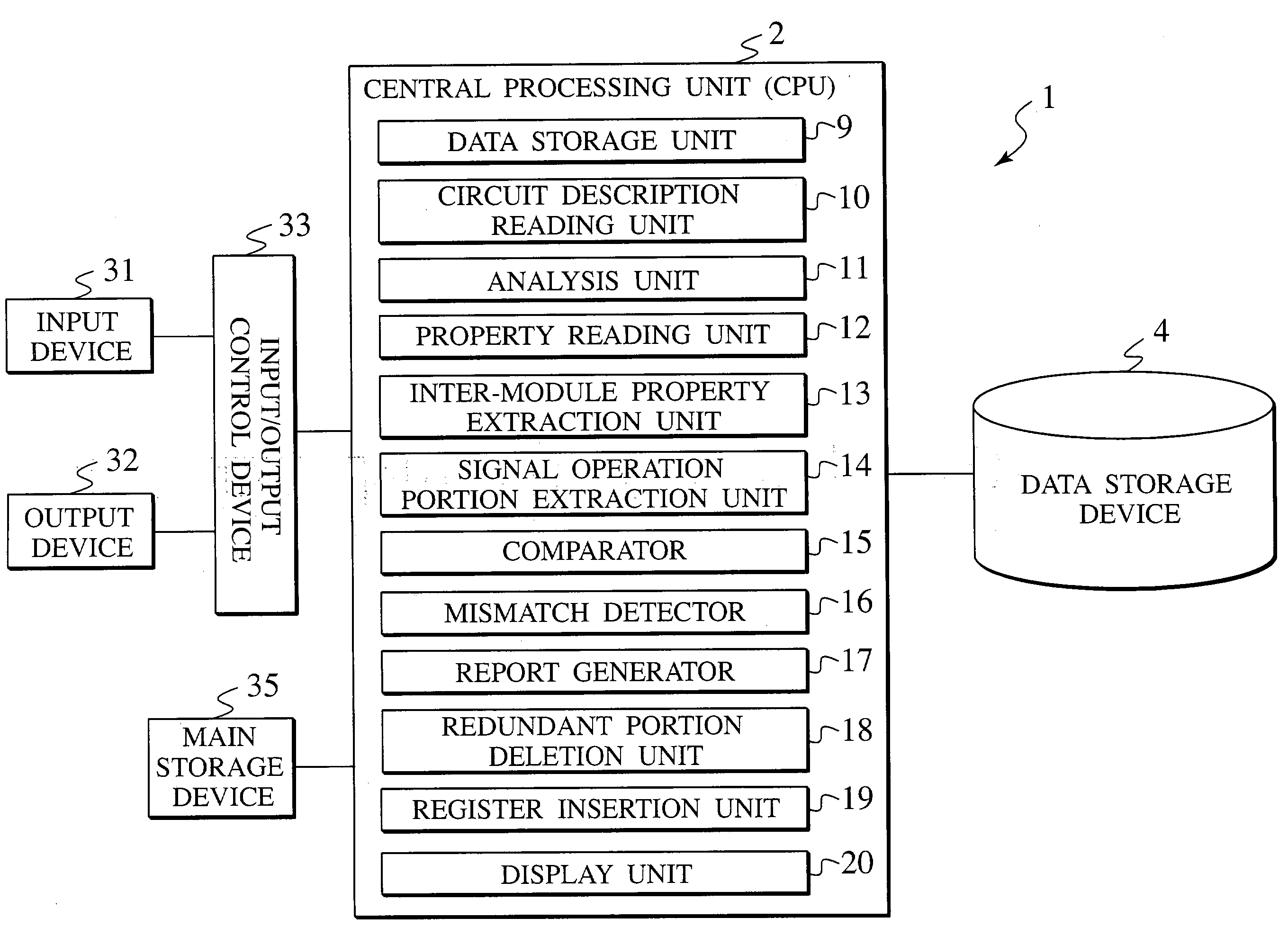
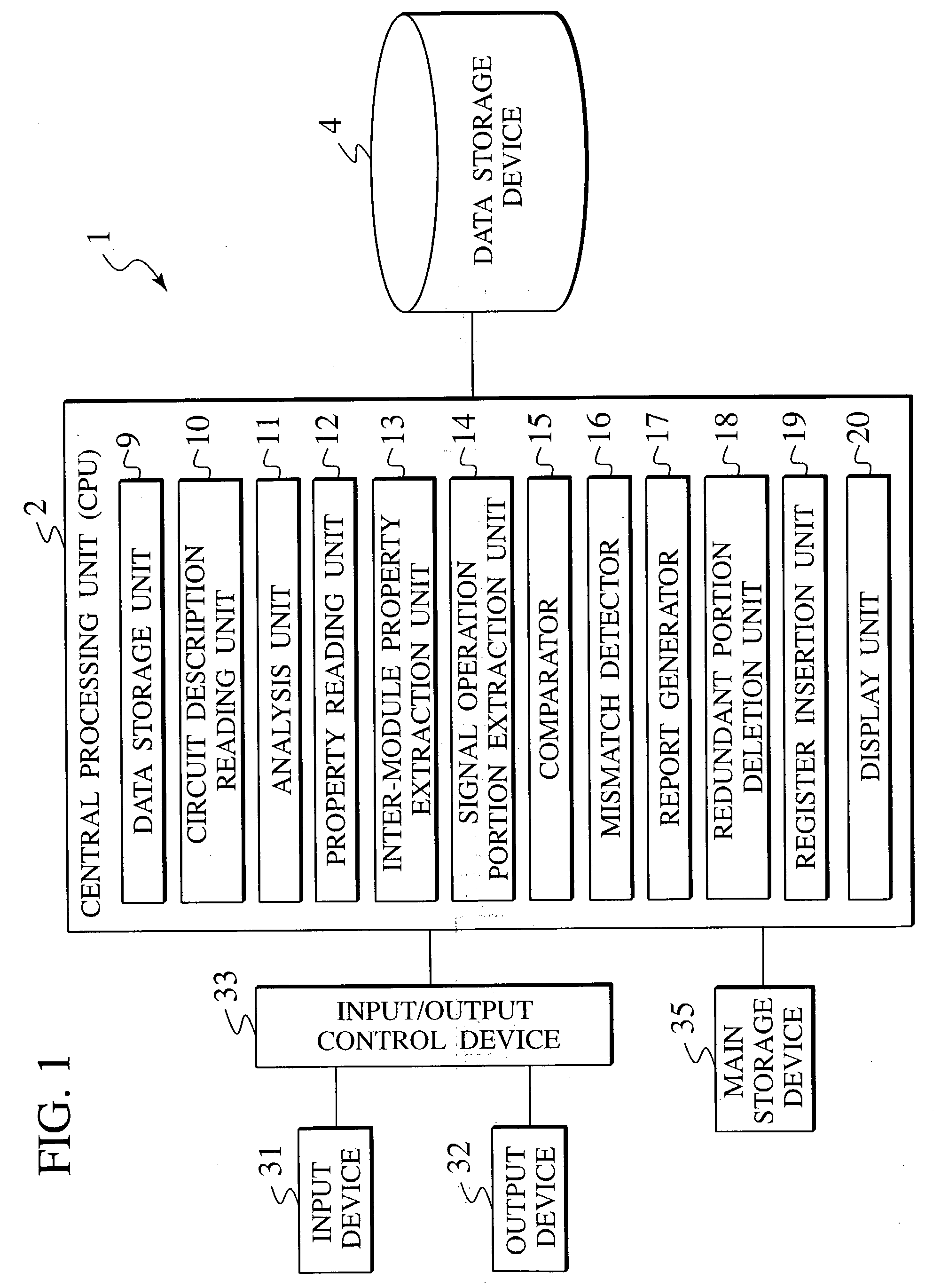
[0076] An LSI design verification apparatus 1 of a first embodiment shown in FIG. 1 includes at least a central processing unit (CPU) 2, an input device 31 and an output device 32 connected through an input / output control device 33 to the CPU 2, a data storage device 4 connected to the CPU 2, and a main memory 35. The CPU 2 is provided with a database management unit for which the drawing is omitted. When an input / output with the data storage device 4 is necessary, a storage place of a necessary file is searched to read out / write the file through this database management unit.

[0077] The CPU 2 includes at least a data storing unit 9, a circuit description reading unit 10, an analysis unit 11, a property reading unit 12, an inter-module property extraction unit 13, a signal operation portion extraction unit 14, a comparator 15, a mismatch detector 16, a report generator 17, a redundant portion deletion unit 18, a register inserti...

second embodiment

[0174] Conceptual Diagram of LSI Design Verification Apparatus

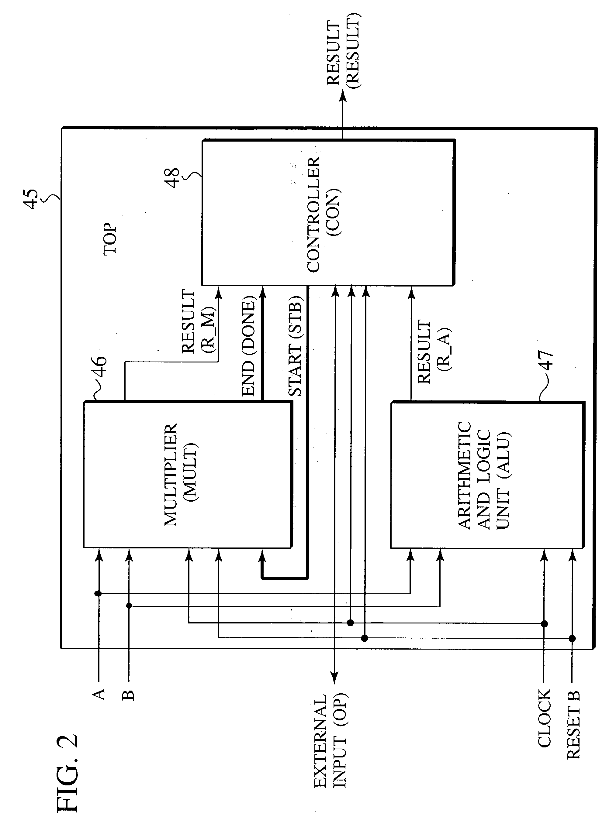
[0175] FIG. 14 shows a conceptual diagram showing an LSI design verification method according to a second embodiment of the present invention. An integrated simulation environment 80 shown in FIG. 14 includes top test bench description (language for verification) 68 in logical simulation, driving test bench description (language for verification) 61 in the logical simulation, expected value checking test bench description (language for verification) 67 in the logical simulation, and top testing model description (HDL) 64 of a verification target module. When a verification target is a module T, first, the verification target module T is analyzed from model description M(TOP) of a top module to obtain an input connection relation (C(I)) of model description of a module I (M(I)) 60 that gives an input to the verification target module T, and an input connection relation (C(T)) of the verification target module T. The drivin...


PUM


Abstract

A computer implemented method for design verification using logical simulation of a circuit description having a plurality of hierarchies from top to bottom in accordance with abstraction of circuit components, which have an arithmetic and logic function, reads the circuit description and analyzes signal connection topologies between the hierarchies of the circuit description from top to bottom. The method stores the data of the signal connection topologies. The method reads properties of target modules implemented by the circuit components in the circuit description. The method extracts a property part having a signal communicating between the target modules. The method extracts an output operation property, defining output operation of an output side module, and an expecting operation property, defining an expecting operation of an input side module among the properties of the target modules. The method compares the output operation properties with the expecting operation properties.

Description

[0001] This application is based upon and claims the benefit of priority from prior Japanese Patent Application P2001-398319 filed on Dec. 27, 2001; the entire contents of which are incorporated by reference herein.[0002] 1. Field of the Invention[0003] The present invention relates to an LSI design verification apparatus, an LSI design verification method, and an LSI design verification program for comparing properties and circuit descriptions which are parts of formal verification.[0004] 2. Description of the Related Art[0005] During a process of designing a semiconductor integrated circuit, there is usually employed a method of representing a circuit configuration to be implemented in the form of a register transfer level (RTL) description and then logically compiling the RTL description into a gate-level netlist. The RTL description corresponds to representation of a circuit configuration, in the form of a description corresponding to a combinational logic gate for implementing ...

Claims


Application Information

Patent Timeline
Patent Type & Authority Applications(United States)
IPC IPC(8): G06F17/50G01R31/28H01L21/82
CPCG06F17/504G06F30/3323
Inventor MATSUOKA, YOSHIKITSUCHIYA, TAKEHIKONISHIDE, TAKEOHORIKAWA, KAZUNARIYANO, EIICHI
Owner KK TOSHIBA
Why Eureka
Try Eureka