

Gas diffussion plate for use in ICP etcher
a technology of diffussion plate and icp etcher, which is applied in the direction of electrical apparatus, electric discharge tube, basic electric elements, etc., can solve the problem of hardly obtaining uniformity of etching process
- Summary
- Abstract
- Description
- Claims
- Application Information
AI Technical Summary
Benefits of technology
Problems solved by technology
Method used
Image

Examples
Embodiment Construction
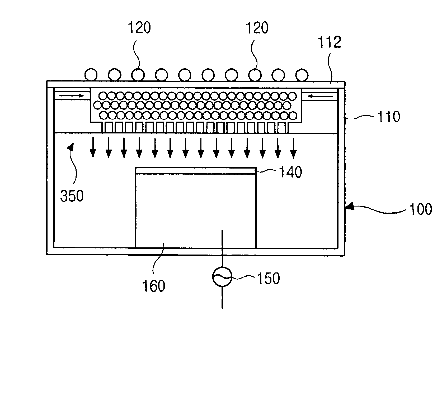
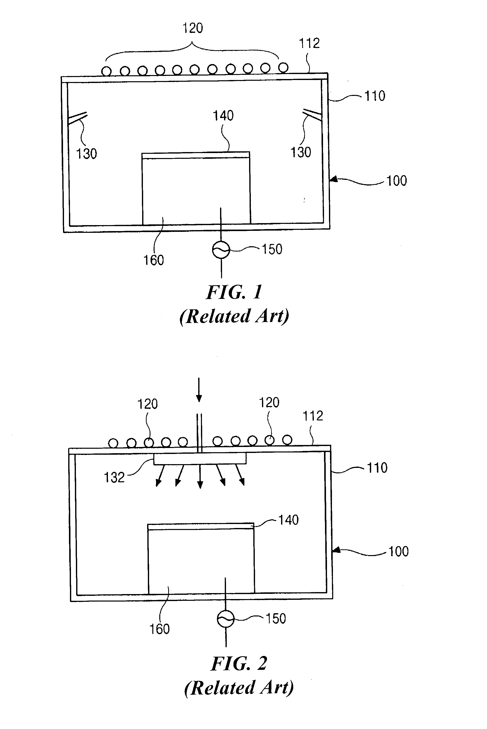
[0027] Reference will now be made in detail to illustrated embodiment of the present invention, examples of which are shown in the accompanying drawings. Wherever possible, the same reference numbers will be used throughout the drawings to refer to the same or similar parts.
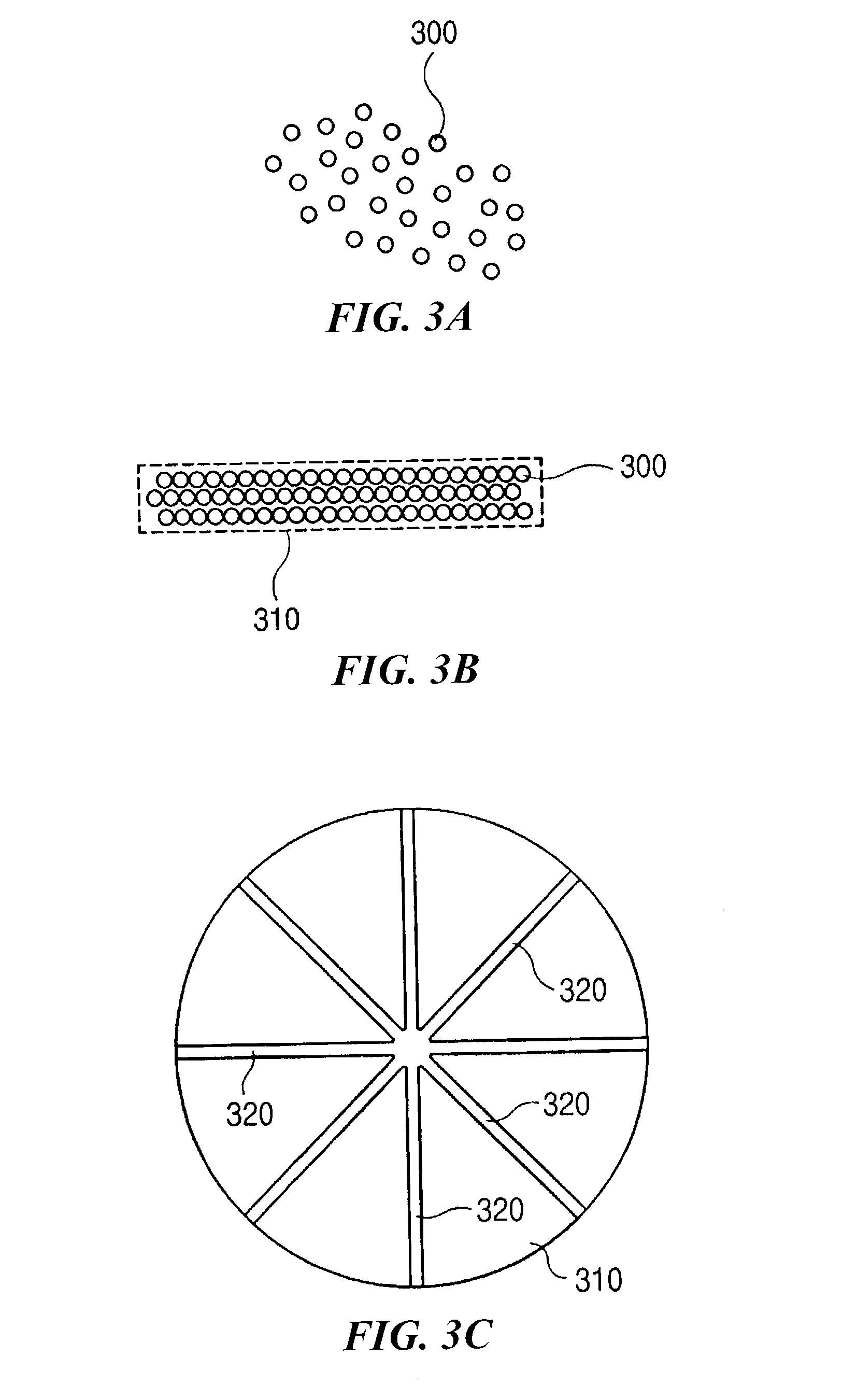
[0028] FIGS. 3A to 3D illustrates a fabrication method for a diffusion plate for use in an ICP etcher according to the present invention.
[0029] In FIG. 3A, a plurality of ceramic balls 300 each having a diameter of about 1 mm are provided. Instead of the ceramic balls 300, a plurality of vespel balls that are a polymer based material can be used. In the present invention, the ceramic or vespel balls have substantially diameters ranging from 0.5 to 5 mm. It is important in the present invention that the material for the gas diffusion plate must not form the polluting particles when the process gases are applied to the ICP etcher. Furthermore, the material for the gas diffusion plate should have heat resistant with...
PUM
| Property | Measurement | Unit |
|---|---|---|
| Diameter | aaaaa | aaaaa |
| Diameter | aaaaa | aaaaa |
| Shape | aaaaa | aaaaa |
Abstract
Description
Claims
Application Information