

Ceramic substrate support
- Summary
- Abstract
- Description
- Claims
- Application Information
AI Technical Summary
Benefits of technology
Problems solved by technology
Method used
Image

Examples
Embodiment Construction
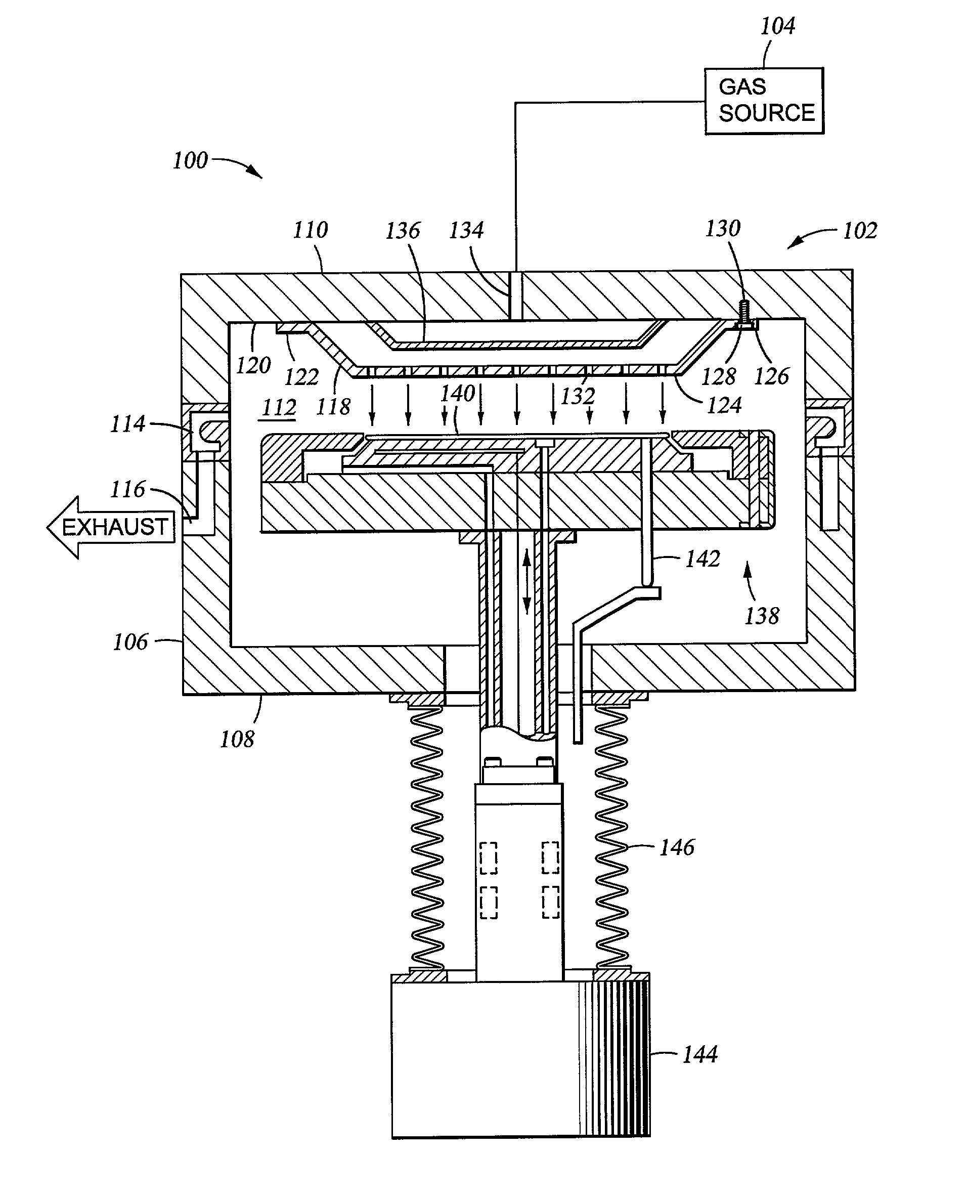
[0030] The present invention generally provides a processing system and heated substrate support that are advantageous for the deposition of tungsten films. The invention is illustratively described below with reference to a chemical vapor deposition system, such as a WxZ.TM. metal chemical vapor deposition (MCVD) system, available from Applied Materials, Inc., of Santa Clara, Calif. However, it should be understood that the invention has utility when depositing other films and in other system configurations such as physical vapor deposition systems, chemical vapor deposition systems and any other system in which supporting a substrate on a ceramic support is desired.
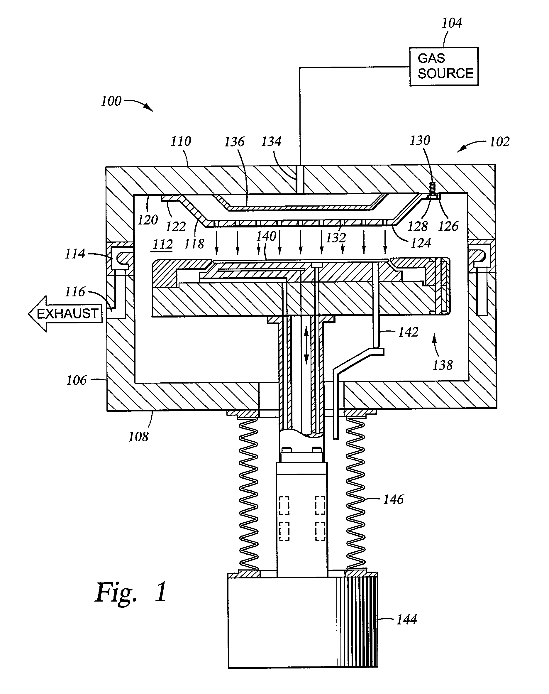
[0031] FIG. 1 is a cross-sectional view of one embodiment of a chemical vapor deposition system 100. The system generally includes a chamber 102 coupled to a gas source 104. The chamber 102 has walls 106, a bottom 108 and a lid 110 that define a process volume 112. The walls 106 and bottom 108 are typically fabricated f...
PUM
| Property | Measurement | Unit |
|---|---|---|
| Vacuum | aaaaa | aaaaa |
| Perimeter | aaaaa | aaaaa |
Abstract
Description
Claims
Application Information