Method for forming charge storage node

Inactive Publication Date: 2003-09-25
SK HYNIX INC
View PDF4 Cites 2 Cited by
  • Summary
  • Abstract
  • Description
  • Claims
  • Application Information

AI Technical Summary

Benefits of technology

[0009] Therefore, a method is disclosed for forming a charge storage node which prevents the bridge between cells and maximizes the hole size of a cell forming portion to thus improve the properties of a device. The disclosed method also increases product yield by depositing an oxide film having a predetermined thickness and forming a contact hole in order to fill the hole of a notch type generated by the etching difference between a damaged sacrificial oxide film and an oxide film for capacitor formation deposited thereon after enlarging the hole size by washing and dipping processes before the formation of the charge storage node.

Problems solved by technology

However, such a conventional method of forming a charge storage node has some defects.
This generates a bridge between cells which deteriorates the operational characteristics of the device and causes a reduction in product yield.

Method used


Image

  • Method for forming charge storage node
  • Method for forming charge storage node
  • Method for forming charge storage node

Examples


Embodiment Construction

[0017] A preferred embodiment will now be described with reference to the accompanying drawings. The preferred embodiment is intended to illustrate the principles of the disclosed methodology, but not to limit the scope of this disclosure.

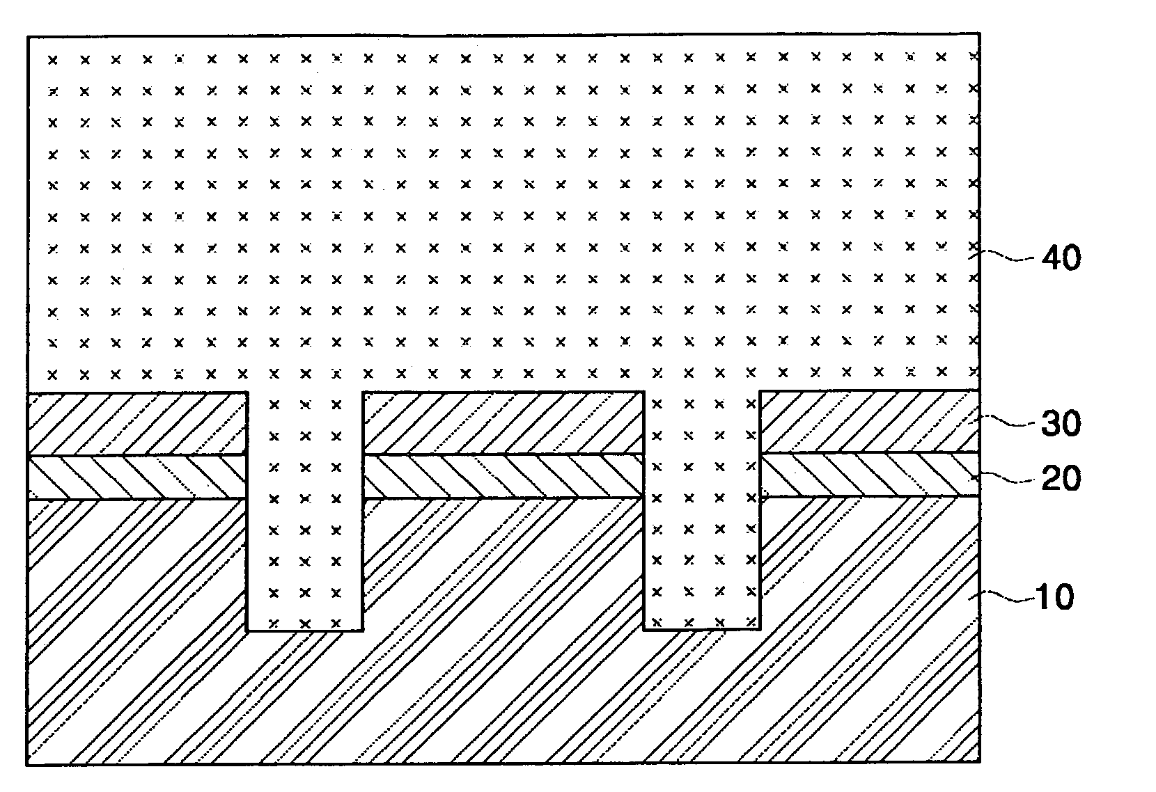
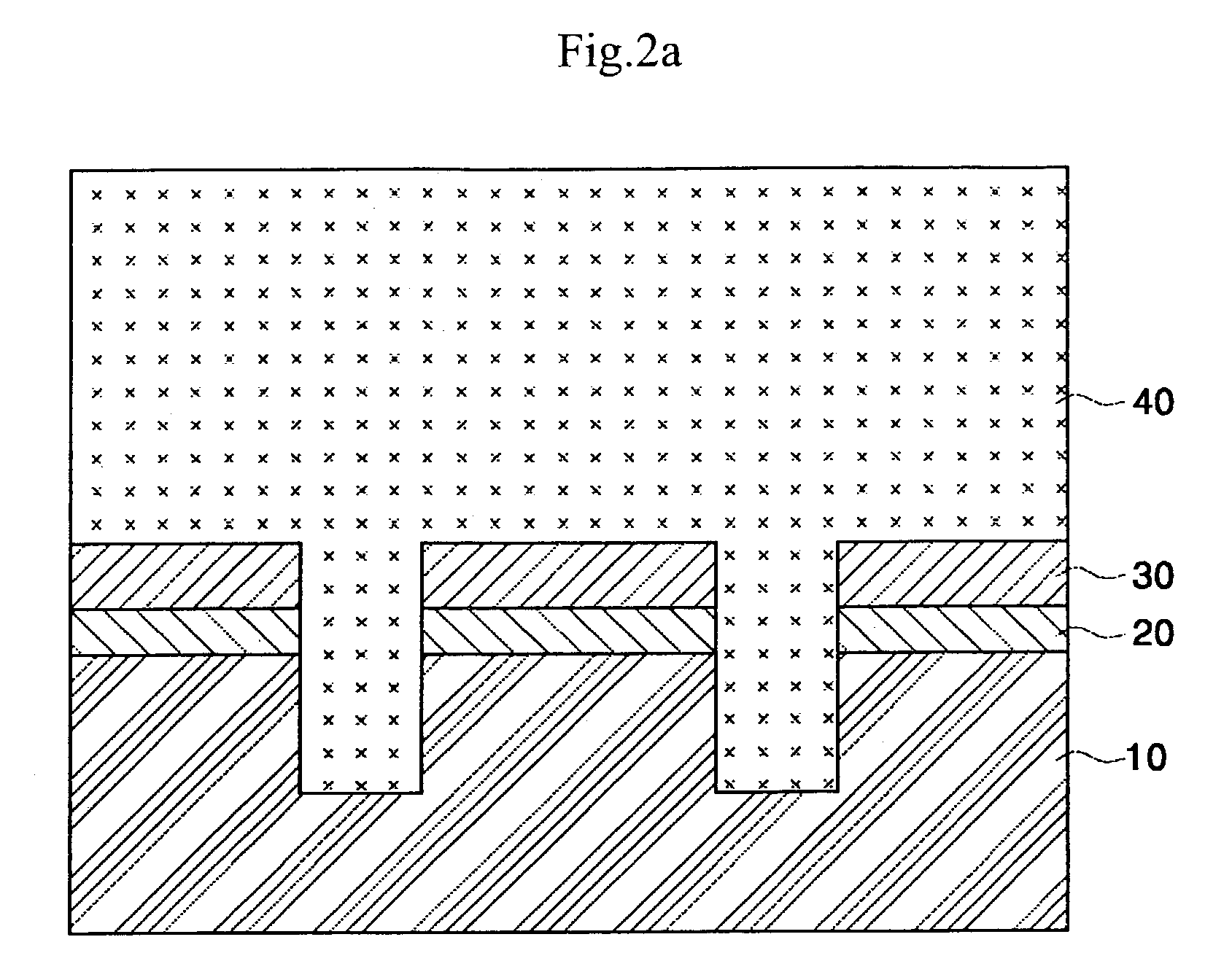
[0018] FIGS. 2a to 2i are cross-sectional views showing a process of forming a charge storage node according to a preferred embodiment.

[0019] Firstly, as illustrated in FIG. 2a, a planarization process is performed to form a charge storage node on a substrate 10 in which a predetermined substructure is formed. Then, an etching stop film 20 and a sacrificial oxide film 30 are deposited in order. Subsequently, a first contact hole (not shown) for the charge storage node is formed by masking and etching processes.

[0020] Next, doped amorphous silicon 40 is deposited to fill the first contact hole (not shown) for the charge storage node.

[0021] Subsequently, as illustrated in FIG. 2b, a second contact hole (B) is formed by an etchback process, and then a...


PUM


Abstract

A method for forming a charge storage node is disclosed. The method for forming a charge storage node prevents the bridge between cells and maximize the hole size of a cell forming portion to thus improve the properties of a device and increase product yield by depositing an oxide film having a predetermined thickness and forming a contact hole in order to fill the hole of a notch type generated by the etching difference between a damaged sacrificial oxide film and an oxide film for capacitor formation deposited thereon after enlarging the hole size by washing and dipping processes before the formation of the charge storage node.

Description

[0001] 1. Technical Field[0002] Methods for forming charge storage nodes are disclosed, and more particularly, methods for forming charge storage nodes which prevent the bridge between cells and maximize the hole size of a cell forming portion to thus improve the properties of the devices and increase product yield by depositing an oxide film having a predetermined thickness and forming a contact hole in order to fill the hole of a notch type generated by the etching difference between a damaged sacrificial oxide film and an oxide film for capacitor formation deposited thereon after enlarging the hole size by washing and dipping processes before the formation of the charge storage node.[0003] 2. Description of the Related Art[0004] Recently, with high integration of semiconductor devices, semiconductor memory devices such as a DRAMs (Dynamic Random Access Memory) demand a capacitance larger than a predetermined capacity to obtain the desired operational characteristics. Also, with h...

Claims


Application Information

Patent Timeline
IPC IPC(8): H01L21/8242H01L21/02H01L21/311H01L21/316H01L27/108
CPCH01L21/31116H01L21/31133H01L28/91H01L27/10855H01L28/84H01L21/31612H10B12/0335H01L21/02164H10B12/00
Inventor WOO, SANG-HOKIM, EUI-SIK
Owner SK HYNIX INC
Why Eureka
Try Eureka