Silicon wafer

Active Publication Date: 2019-04-25
GLOBALWAFERS JAPAN
View PDF10 Cites 0 Cited by
  • Summary
  • Abstract
  • Description
  • Claims
  • Application Information

AI Technical Summary

Benefits of technology

[0017]The silicon wafer according to the present invention comprises a denuded zone (DZ layer) which includes a surface of the silicon wafer and of which the density of vacancy-oxygen complexes (VOx) which comprise complexes of vacancies and oxygen is less than 1.0×10¹²/cm3; an intermediate layer disposed inwardly, in the depth direction of the silicon wafer, of the denuded zone so as to be adjacent to the denuded zone, wherein the density of the vacancy-oxygen complexes in the intermediate layer increases gradually inwardly in the depth direction from the boundary with the denuded zone within a range of 1.0×10¹²/cm3 or over and less than 5.0×10¹²/cm3, the intermediate layer having a depth tI determined corresponding to t

Problems solved by technology

However, an infrared light scattering tomography apparatus is capable of detecting only oxygen precipitates of 25 nm in size or over, and is incapable of detecting any smaller oxygen precipitates.
On the other hand, it is known that in semiconductor devices for an image sensor, oxygen precipitates that are smaller in size than the lower detection limit of an inf

Method used


Image

  • Silicon wafer
  • Silicon wafer
  • Silicon wafer

Examples


Embodiment Construction

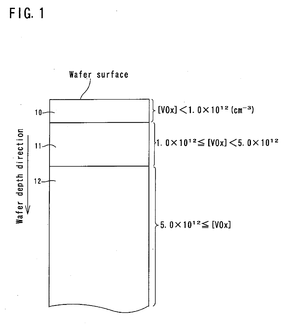
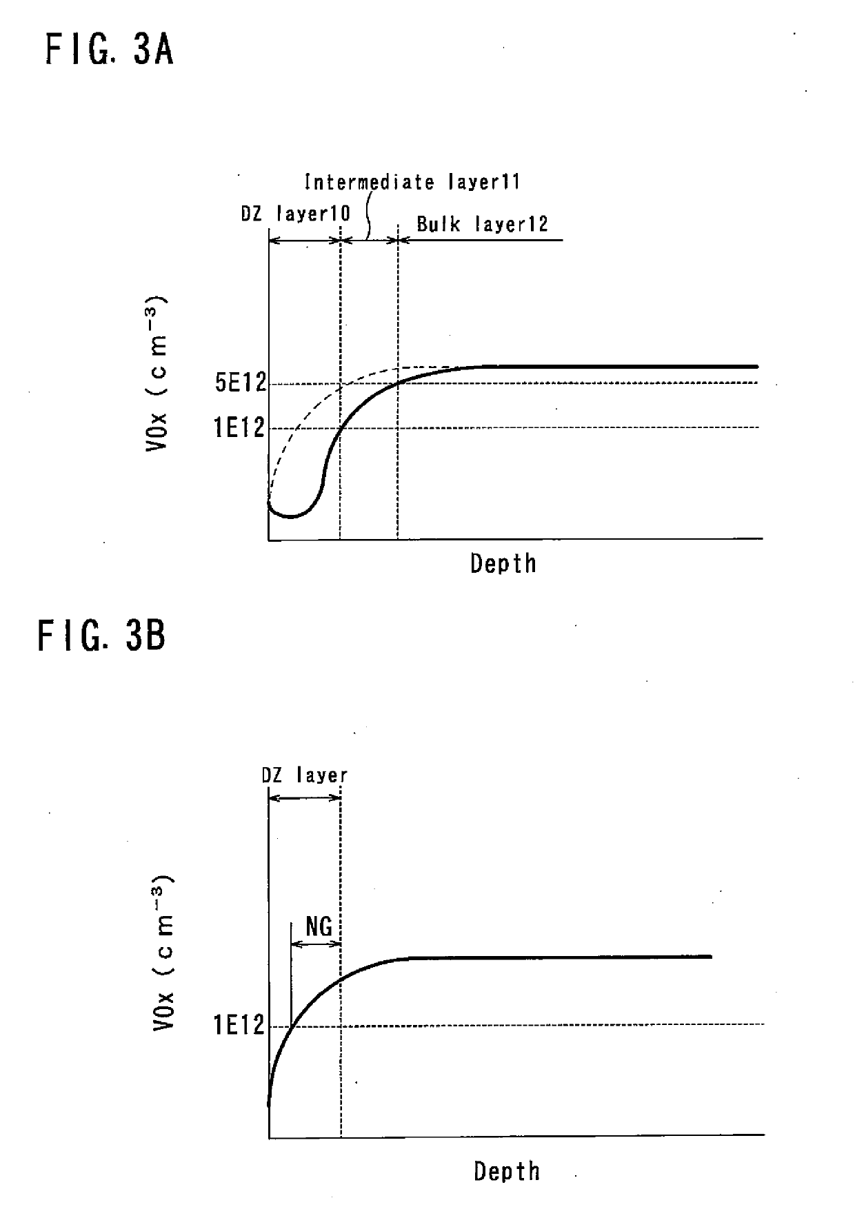
[0036]FIG. 1 shows a vertical sectional view of the silicon wafer (hereinafter simply referred to as the “wafer”) according to the present invention. This wafer is sliced from an ingot grown by the Czochralski process. A mirror-finishing its both sides, it is subjected to a rapid thermal process (RTP) comprising the below-described heat treatment sequence (shown in FIG. 4). The wafer has a surface layer comprising a denuded zone (hereinafter referred to as the “DZ layer”) 10 of which the density of the vacancy-oxygen complexes (VOx), i.e., the complexes of vacancies and oxygen, is less than 1.0×10¹² / cm3. The depth of the DZ layer is determined corresponding to the kind of semiconductor devices formed on the wafer, and is typically within the range of 3-100 μm.

[0037]By limiting the VOx density of the DZ layer to less than 1.0×10¹² / cm3, oxygen precipitates, which could deteriorate the device properties, will not precipitate in the DZ layer 10 during the device manufacturing process. T...


PUM


Abstract

A silicon wafer includes a denuded zone which is a surface layer and of which the density of vacancy-oxygen complexes which are complexes of vacancies and oxygen is less than 1.0×10¹²/cm3. An intermediate layer is disposed inwardly of the denuded zone so as to be adjacent to the denuded zone. The density of the vacancy-oxygen complexes in the intermediate layer increases gradually inwardly in the depth direction from the boundary with the denuded zone within a range of 1.0×10¹²/cm3 or over and less than 5.0×10¹²/cm3. The intermediate layer has a depth determined corresponding to the depth of the denuded zone. A bulk layer is disposed inwardly of the intermediate layer so as to be adjacent to the intermediate layer. The density of the vacancy-oxygen complexes in the bulk layer is 5.0×10¹²/cm3 or over.

Description

TECHNICAL FIELD[0001]The present invention relates to a silicon wafer having a surface layer in which semiconductor devices are formed.BACKGROUND ART[0002]With an increasing degree of integration and increasing performance of today's semiconductor devices, higher quality is required for silicon wafers (hereinafter simply referred to as “wafers”) used as substrates for semiconductor devices.[0003]Specifically, it is required that a denuded zone (hereinafter referred to as the “DZ layer”), which forms the surface layer of the wafer in which semiconductor devices are formed, is completely free of oxygen precipitates which are compounds of silicon and oxygen that dissolves into the silicon crystal during growth of the silicon crystal from a crucible for storing silicon melt, and also completely free of void defects which are aggregates of vacancies introduced into the crystal during growth of the crystal. This is because oxygen precipitates could act as leak current sources and deterior...

Claims


Application Information

Patent Timeline
IPC IPC(8): C30B29/06C30B33/02H01L21/322H01L21/324
CPCC30B29/06C30B33/02H01L21/3225H01L21/324H01L21/322H01L31/02363H01L21/02002H01L21/02112
Inventor MAEDA, SUSUMUBANBA, HIRONORISUDO, HARUOOKAMURA, HIDEYUKIARAKI, KOJISUEOKA, KOJINAKAMURA, KOZO
Owner GLOBALWAFERS JAPAN
Why Eureka
Try Eureka