Vertical organic transistor and method of fabricating the same

a vertical organic transistor and transistor channel technology, applied in the direction of thermoelectric device junction materials, electrical equipment, semiconductor devices, etc., can solve the problems of low resolution and frame rate, low mobility of organic semiconductor serving as transistor channel, and most attempts to fabricate an n-type organic semiconductor have not achieved a breakthrough, so as to enhance the output current and the ion/ion off rate of the vertical transistor

Inactive Publication Date: 2007-08-02
IND TECH RES INST
View PDF1 Cites 4 Cited by
  • Summary
  • Abstract
  • Description
  • Claims
  • Application Information

AI Technical Summary

Benefits of technology

[0010] Accordingly, the object of the present invention is to provide a vertical organic transistor and the method of fabricating the same, suitable for enhancing the output current and the Ion / Ioff rate of the vertical transistor.

Problems solved by technology

However, since organic electronic devices have bottlenecks in device properties, even flat panel displays will generally experience problems of low resolution and frame rate, let alone the application of organic transistor devices that operate at Mega Hertz (MHz) and above.
The mobility of the organic semiconductor serving as a transistor channel is too low.
Therefore, most attempts to fabricate an N type organic semiconductor have achieved no breakthrough.
It is too difficult to be integrated into a mature fabricating process.
Since most organic semiconductor materials can easily reacted with chemicals commonly used in the semiconductor industry and changed, conventional fabrication methods cannot be adopted in preparing such organic semiconductor materials.
And after this fabricating process, further fabricating processes for enhancing device properties can not be performed.
Therefore, most research of organic transistors is currently limited to simple bottom gate / source / drain contact layer / organic semiconductors or a bottom gate / organic semiconductor / source / drain contact layer structure.
Thus, not only are the device properties limited, but the research of complex hetero structures is also held back.
However, because it is difficult to hold the material properties of the vertical organic transistor, device properties such as the output current and lon / loff rate of the transistor are not good enough.

Method used


Image

  • Vertical organic transistor and method of fabricating the same
  • Vertical organic transistor and method of fabricating the same
  • Vertical organic transistor and method of fabricating the same

Examples


Embodiment Construction

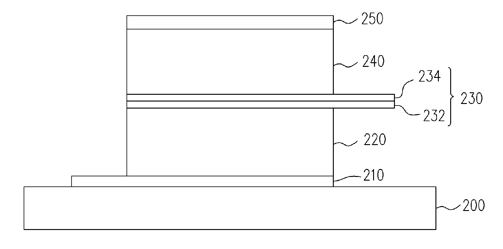
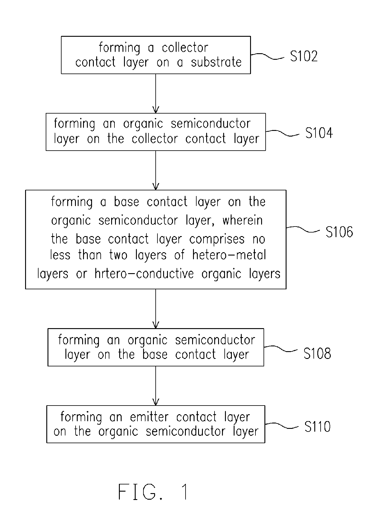
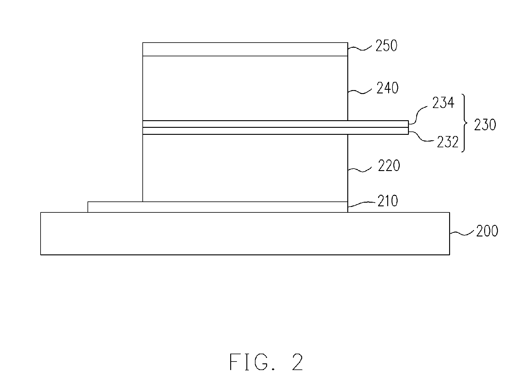
[0028]FIG. 1 is a flowchart of fabricating a vertical organic transistor of the preferred embodiment of the present invention. And FIG. 2 is a schematic cross-sectional view of a vertical organic transistor of the preferred embodiment of the present invention.

[0029] First, referring to step S102 of FIG. 1 and FIG. 2, a collector contact layer 210 is formed on a substrate 200. The method of forming the collector contact layer 210 involves, for example, using a metal shadow mask with a desired pattern to form the collector contact layer 210 on the substrate 200 by vacuum deposition, ink jet, screen printed method, spin-coating, or the like. And the substrate 200 is, for example, a glass substrate, a plastic substrate, or a flexible substrate. The collector contact layer 210 is, for example, a metal layer or a conductive organic layer. In the present embodiment, the collector contact layer 210 is, for example, a gold metal layer with a thickness of 10 nm.

[0030] Then, referring to ste...


PUM


Abstract

A vertical organic transistor is disclosed, which includes at least: a collector contact layer disposed on a substrate; a first organic semiconductor layer disposed on the collector contact layer; a base contact layer disposed on the first organic semiconductor layer, wherein the base contact layer comprises no less than two layers of hetero-metal layers or hetero-conductive organic layers; a second organic semiconductor layer disposed on the base contact layer; and an emitter contact layer disposed on the second organic semiconductor layer. Device properties such as output current and Ion/Ioff rate can be improved by using the vertical organic transistor of this invention.

Description

CROSS-REFERENCE TO RELATED APPLICATION [0001] This application claims the priority benefit of Taiwan application serial no. 95103384, filed on Jan. 27, 2006. All disclosure of the Taiwan application is incorporated herein by reference. BACKGROUND OF THE INVENTION [0002] 1. Field of Invention [0003] The present invention relates to a vertical organic transistor and a method of fabricating the same. More particularly, the present invention relates to a vertical organic transistor having a base contact layer made of no less than two hetero materials and a method of fabricating the same. [0004] 2. Description of Related Art [0005] Compared with conventional inorganic electronic devices (Si- and GaAs-based electronic devices), the most striking feature of organic electronic devices is low dependency on the substrate. That is, an organic electronic device can be fabricated on a flexible substrate and applied in fabricating a flexible flat panel display. And a low-priced printing technique...

Claims


Application Information

Patent Timeline
Patent Type & Authority Applications(United States)
IPC IPC(8): H01L29/08
CPCH01L51/0504H01L51/057H01L51/0508H10K10/00H10K10/46H10K10/491
Inventor LIN, SHIH-YENOU, TZU-MINYANG, CHUAN-YICHOU, SHU-TINGHUANG, CHUN-YUANCHAN, I-MINCHENG, SHIAU-SHINCHAN, YI-JEN
Owner IND TECH RES INST
Why Eureka
Try Eureka