Method for forming wafer

a technology of silicon substrate and forming method, which is applied in the field of semiconductor manufacturing, can solve the problems of hot carrier effect degradation, reduced microelectronic device size, and increased silicon substrate quality, and achieves the effects of reducing the surface roughness of silicon substrate, preventing carrier penetration, and enhancing device properties

Inactive Publication Date: 2017-04-13
ZING SEMICON CORP
View PDF5 Cites 0 Cited by
  • Summary
  • Abstract
  • Description
  • Claims
  • Application Information

AI Technical Summary

Benefits of technology

[0020]The method of the present application is advantageous over the prior art. After forming the silicon substrate, the rapid thermal annealing is performed to the substrate to form the passivation layer. The passivation layer is able to reduce the surface roughness of the silicon substrate. Further, during the formation of a gate oxide layer or an interface, deuterium can diffuse from the substrate and combine with dangling bonds of the interface to form a stable structure, thereby the carrier penetration can be prevented and the device properties can be enhanced.

Problems solved by technology

Challenges for the quality of the silicon substrate are increasing with the tendency of size reduction of microelectronic devices.
Another problem which has arisen in the semiconductor industry is the degradation of device performance by hot carrier effects.
Therefore, the dangling bond is exposed again to adversely affect the properties of the device.

Method used


Image

  • Method for forming wafer

Examples


Embodiment Construction

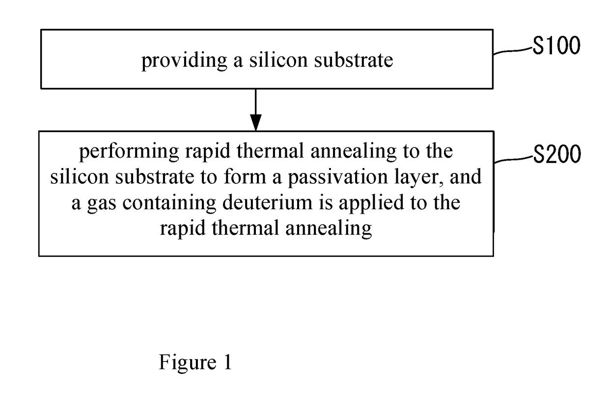
[0022]Although the following with reference to the accompanying drawings of the method of the present invention is further described in more detail, there is shown a preferred embodiment of the present invention. A person having ordinary skills in the art may modify the invention described herein while still achieving the advantageous effects of the present invention. Thus, these embodiments should be understood as broad teaching one skilled in the art, and not as a limitation of the present invention.

[0023]For purpose of clarity, not all features of an actual embodiment are described. It may not describe the well-known functions as well as structures in detail to avoid confusion caused by unnecessary details. It should be considered that, in the developments of any actual embodiment, a large number of practice details must be made to achieve the specific goals of the developer, for example, according to the requirements or the constraints of the system or the commercials, one embod...


PUM

PropertyMeasurementUnit
temperatureaaaaaaaaaa
sizeaaaaaaaaaa

Abstract

This invention provides a method for forming a wafer comprising forming a silicon substrate, and then performing rapid thermal annealing to the substrate to form a passivation layer. The passivation layer reduces the surface roughness of the silicon substrate. During the formation of a gate oxide layer or an interface, deuterium can diffuse from the substrate and combine with dangling bonds of the interface to form a stable structure, thereby carrier penetration can be prevented and device properties can be enhanced.

Description

BACKGROUND OF THE INVENTION[0001]1. Field of the Invention[0002]The present application relates to a semiconductor manufacture, and more particularly to a method of formation of a wafer.[0003]2. Description of the Related Art[0004]Monocrystalline silicon is the initial material in the semiconductor manufacture, which is generally formed by Czochralski (CZ) method.[0005]Challenges for the quality of the silicon substrate are increasing with the tendency of size reduction of microelectronic devices. The quality of the silicon substrate depends on size and distribution of microdefects grown therein. During the formation of the silicon substrate by CZ method or float zone method, most of the microdefects clusters among the silicon-vacancies or fills within the spaces.[0006]Hydrogen passivation has become a well-known and established practice in the fabrication of semiconductor devices. In the hydrogen passivation process, defects which affect the operation of semiconductor devices are r...

Claims


Application Information

Patent Timeline
Patent Type & Authority Applications(United States)
IPC IPC(8): H01L21/30B24B9/06B24B7/22
CPCH01L21/3003B24B9/065B24B7/228
Inventor XIAO, DEYUANCHANG, RICHARD R.
Owner ZING SEMICON CORP
Why Eureka
Try Eureka