
Method of preventing seam defects in isolated lines

a technology of isolated lines and seam defects, applied in the direction of basic electric elements, semiconductor/solid-state device manufacturing, electric devices, etc., can solve the problem of severe seam defect problem, and achieve the effect of uniform planarization rate and prevent seam defects

Inactive Publication Date: 2003-10-23
TEXAS INSTR INC
View PDF0 Cites 39 Cited by
  • Summary
  • Abstract
  • Description
  • Claims
  • Application Information

AI Technical Summary

Benefits of technology

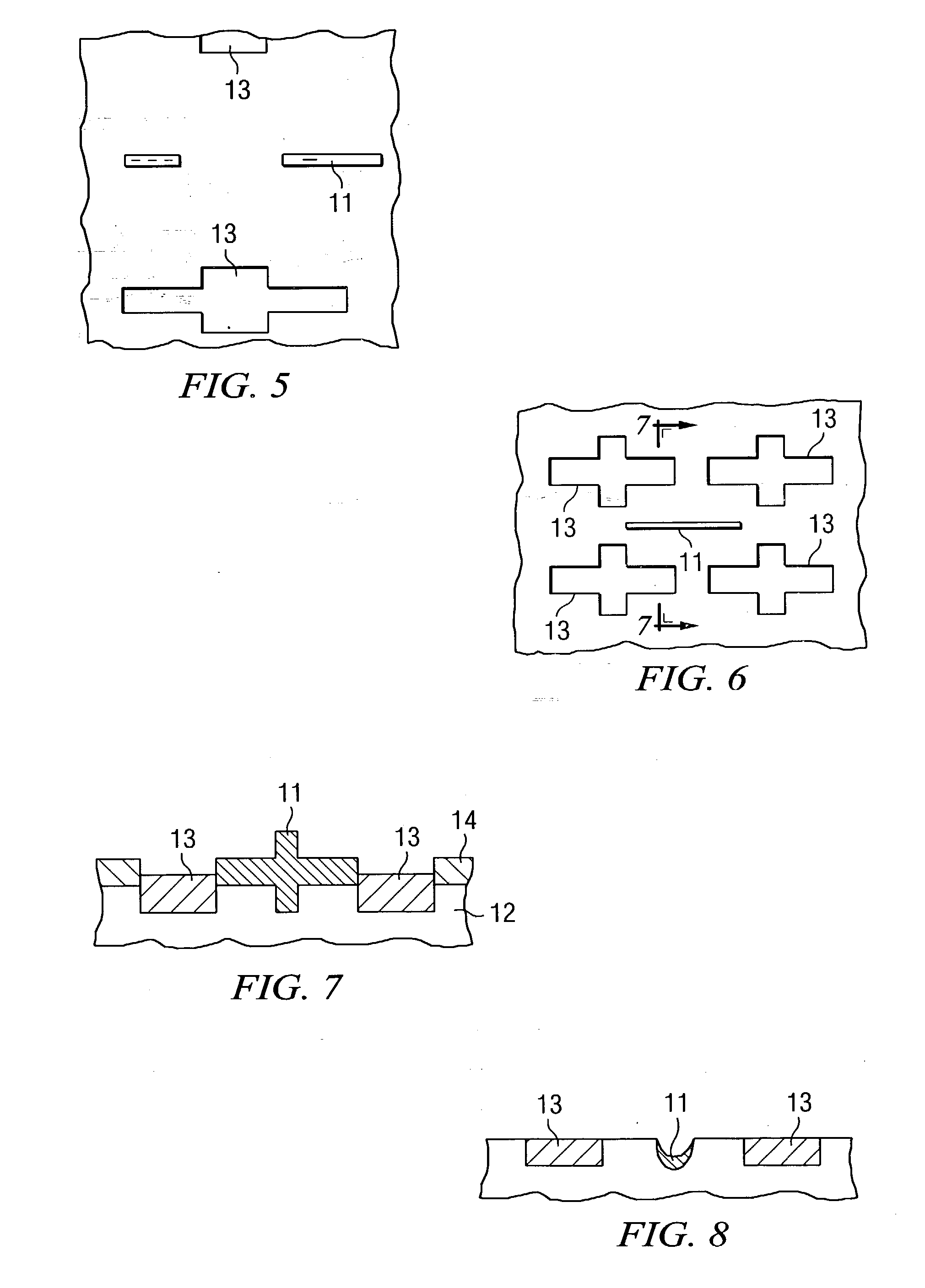
[0006] In accordance with one embodiment of the present invention, the shape, size, and density of the dummy metal structures are designed specifically when are used to surround narrow, isolated lines so that homogeneous metal density distribution across the area promotes uniform planarization rate, and consequently prevents seam defects.
[0007] In accordance with another embodiment of the present invention a method of preventing seam defects on narrow, isolated lines in the active region during CMP process with dummy metal structures includes providing with the narrow, isolated line dummy metal structures with features thereof of widths to have fill up rates that match the narrow, isolated line with a certain density of said dummy metal structures on the semiconductor device

Problems solved by technology

A severe seam defect problem has been observed at post CMP defect inspection.
The problem occurs specifically in features that are narrow, isolated and electrically floating after the polishing is complete.

Method used


Image

  • Method of preventing seam defects in isolated lines
  • Method of preventing seam defects in isolated lines
  • Method of preventing seam defects in isolated lines

Examples


Embodiment Construction

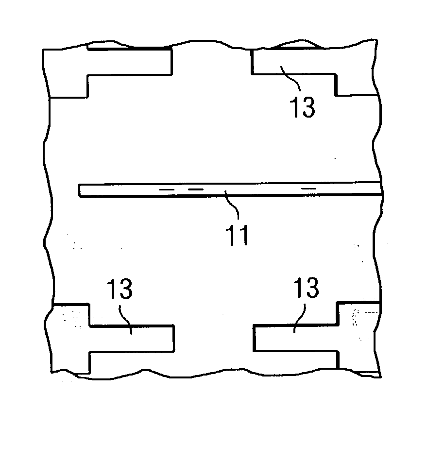
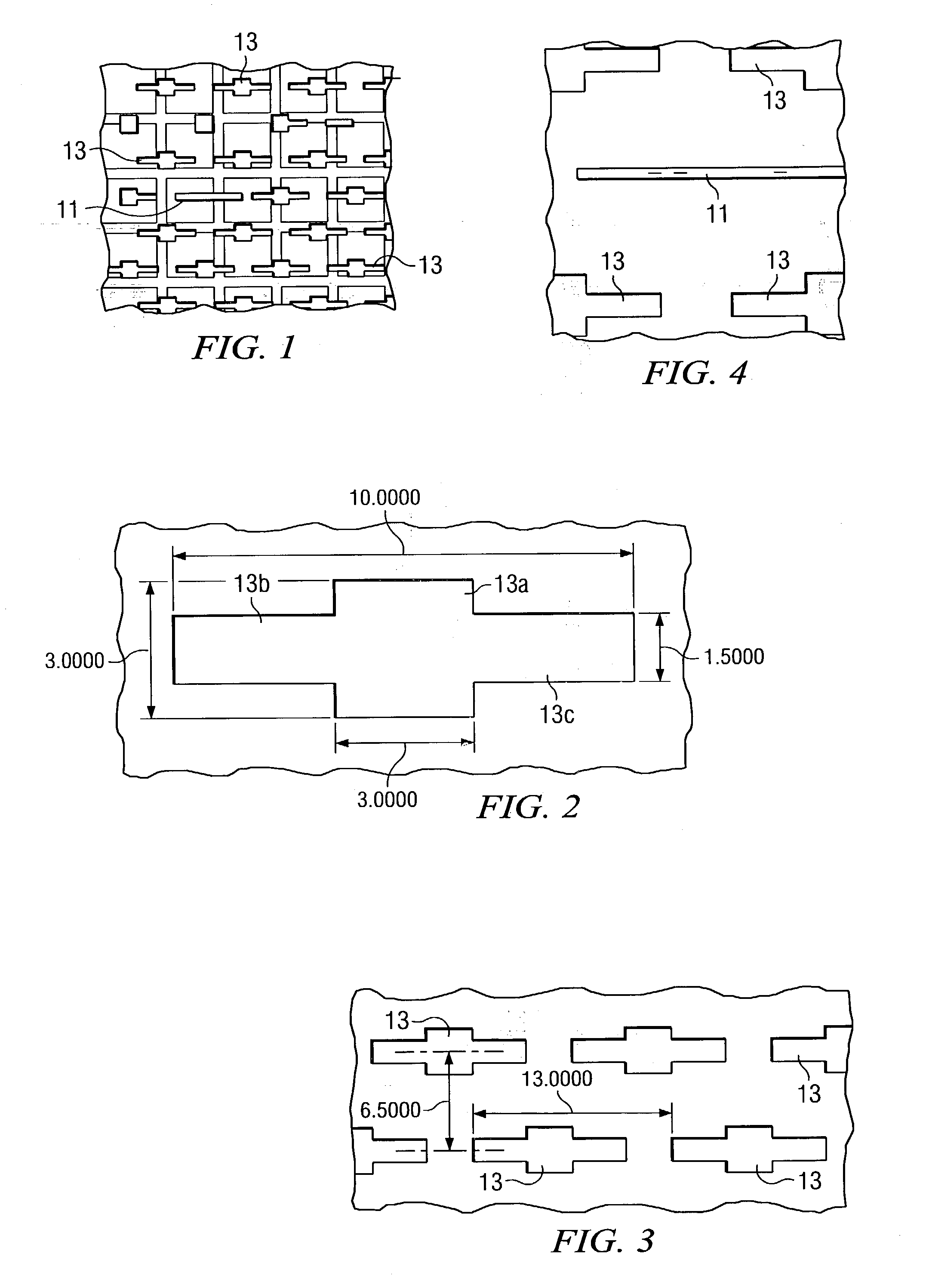
[0020] FIG. 1 illustrates a narrow, isolated interconnect line 11 surrounded by dummy metal structures 13. The term narrow line herein refers to lines that are 0.3 microns or less in width. The term isolated line refers to lines 1.5 microns from the nearest other line. FIG. 2 illustrates the size and shape of a preferred prior art dummy metal structure 13 used by Tex. Instruments Inc. The dummy metal structure 13 has a square center portion 13a and two thinner wings or arms 13b and 13c extending in opposite directions from the center portion 13a. The long dimension including the center portion 13a and the wings 13b and 13c is 10 microns. The broad center portion 13a is 3.times.3 micron and the narrow wings are each 3.5 microns long and 1.5 microns wide. The vertical pitch of the dummy metal structures as illustrated in FIG. 3 is 6.5 microns and the horizontal pitch is 13 microns between structures. The structures and pitches are selected to present uniform capacitance to active line...


PUM


Abstract

A method of preventing seam defects on narrow, isolated lines of 0.3 micron or less during CMP process is provided. The solution is to change the size of features of dummy metal structures on the same layer as the metal layer to have a width that is about 0.6 micron or less so that during the electroplating the deposition rate in the features is similar to the narrow, isolated lines. The density, shape, and proximity of the dummy metal structures further prevents the seam defects during CMP processing by preventing Galvanic corrosion.

Description

[0001] This application is a continuation-in-part application of application Ser. No. 10 / 123528 filed Apr. 17, 2002. entitled "Method of Preventing Seam Defects In Isolated Lines." This application is incorporated herein by reference.[0002] This invention relates to semiconductor devices utilizing copper metallization, particularly to Chemical Mechanical Planarization (CMP) of copper interconnect lines, and to preventing seam defects in narrow, isolated metal lines.BACKGROUND OF INVENTION[0003] The manufacturing of semiconductor devices often includes layers of electrical circuits and / or dielectric on top of a semiconductor substrate. The electrical circuits often include narrow, isolated conductive interconnect lines circuits on one or more layers on the semiconductor substrate. The one or more layers of electrical lines and / or dielectric layers undergo Chemical Mechanical Polishing (CMP). The polishing polishes excess metal in a damascene process where holes are formed in a dielec...

Claims


Application Information

Patent Timeline
IPC IPC(8): H01L21/321H01L21/768
CPCH01L21/3212H01L21/7684H01L21/76838
Inventor PERMANA, DAVIDLU, JIONG-PINGCHENG, ALBERTWEST, JEFF A.FAIRCHILD, BROCK W.JOHANNESMEYER, SCOTT A.BOWLES, CHRIS M.BONIFIELD, THOMAS D.TIWARI, RAJESH
Owner TEXAS INSTR INC
Learn More