Vertical semiconductor device with tunnel insulator in current path controlled by gate electrode

a tunnel insulator and gate electrode technology, applied in semiconductor devices, digital storage, instruments, etc., can solve the problems of deteriorating leakage current generation between source and drain, and serious problems such as leakage to the substrate, and the resistance of diffusion layers to deteriorate the driving force of transistors,

Inactive Publication Date: 2003-11-13
HITACHI LTD
View PDF4 Cites 54 Cited by
  • Summary
  • Abstract
  • Description
  • Claims
  • Application Information

AI Technical Summary

Problems solved by technology

However, as the source-drain distance becomes shorter, with only the barrier it is no longer possible to effect the isolation to a satisfactory extent, and the problem of leakage to the substrate and that of generation of leakage current between source and drain have become serious problems.
However, shallowing the depth of the diffusion layers gives rise to the problem that the resistance of the diffusion layers increases to deteriorate the driving force of the transistor.
In this structure, it is possible to suppress the leakage current without increasing the diffusion layer resistance, but it is necessary to let a channel current flow through an insulating film, thus giving rise to the problem that the driving force is deteriorated.
However, it is difficult to form a sufficient junction in comparison with PN junction, with consequent increase in the leakage to the substrate and cancellation of the source-drain leakage reducing effect.
Thus, the bottom is a main source of current leakage.

Method used


Image

  • Vertical semiconductor device with tunnel insulator in current path controlled by gate electrode
  • Vertical semiconductor device with tunnel insulator in current path controlled by gate electrode
  • Vertical semiconductor device with tunnel insulator in current path controlled by gate electrode

Examples


Embodiment Construction

[0079] Prior to a concrete description of embodiments of the present invention, main modes for carrying out the invention will be outlined below.

[0080] Semiconductor Device According to the Invention

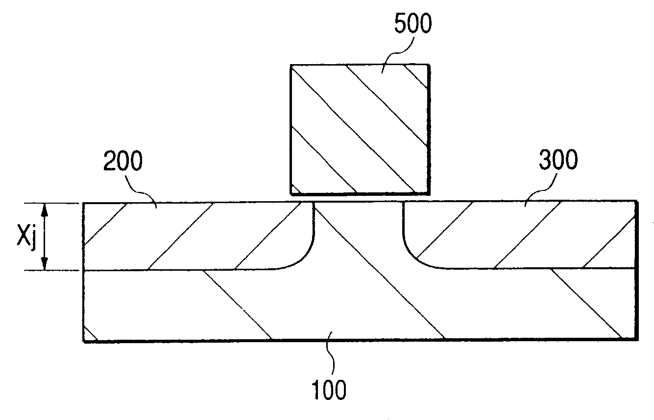
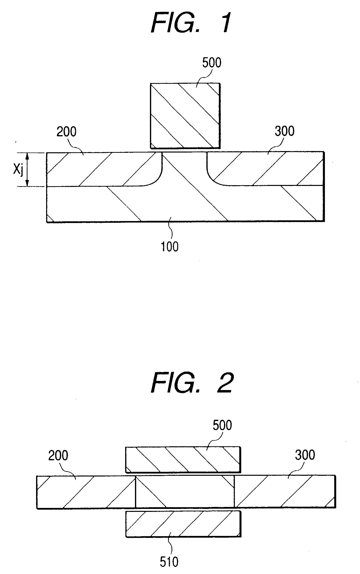
[0081] A typical first mode of the present invention resides in a semiconductor device comprising a semiconductor region, the semiconductor region having a first conductive region, a first insulating film, a first semiconductor region, and a second conductive region; a second insulating film formed at least in the first semiconductor region; and a third conductive region formed on the surface of the second insulating film.

[0082] The present invention can provide a novel switching device, which is extremely useful as a switching portion in the novel semiconductor device as will be described later. The structure of the invention can be manufactured by a conventional manufacturing method adopted in the semiconductor field. Thus, the semiconductor device in question can be provided in an ext...


PUM


Abstract

It is an object of the present invention to provides a field effect transistor with extremely low leakage current. It is another object of the invention to provide a semiconductor memory device having an excellent information holding characteristic. It is a further object of the invention to provide a method for manufacturing in a simple manner a novel field effect transistor or semiconductor memory device with extremely low leakage current. According to a typical basic configuration of the present invention, a thin insulating film is inserted in a vertically disposed Schottky junction to form source and drain electrodes and a tunnel of the insulating film in the junction is controlled by a gate electrode. The gate electrode is disposed on each of both sides of a vertical channel, permitting a field effect to be exerted effectively on the junction, whereby a junction leakage in an OFF state can be made extremely low.

Description

[0001] 1. Field of the Invention[0002] The present invention relates to a semiconductor device capable of being integrated on a large scale and a semiconductor memory device using the semiconductor device. The present invention is further concerned with a manufacturing method for the semiconductor device or the semiconductor memory device.[0003] 2. Related Arts[0004] A principal portion of a ULSI transistor using a silicon substrate, which is a typical up-to-date integrated semiconductor device, has such a sectional structure as shown in FIG. 1. In the same figure, the transistor used in a CMOS is constituted by an insulated gate transistor which uses diffusion layers (200, 300) heavily doped with impurity as source and drain electrode regions on a semiconductor substrate 100. The reference numeral 500 denotes a gate electrode.[0005] A MOSFET, which is a typical example of an insulated gate transistor, uses only a different conductive type carrier as a carrier in a channel to be con...

Claims


Application Information

Patent Timeline
Patent Type & Authority Applications(United States)
IPC IPC(8): G11C11/404H01L21/8234H01L21/8242H01L27/06H01L27/108H01L27/12H01L29/08
CPCG11C11/404H01L21/823487H01L27/0688H01L29/0895H01L27/10823H01L27/10876H01L27/1203H01L27/108H10B12/34H10B12/00H10B12/053
Inventor HISAMOTO, DAIKATAYAMA, KOZA
Owner HITACHI LTD
Why Eureka
Try Eureka