Thin film transistor

a thin film transistor and transistor technology, applied in the direction of transistors, semiconductor devices, electrical equipment, etc., can solve the problems of instability of tft characteristics, difficult to obtain constant amount of doped impurity ions by varying the energy of doping impurity ions into the gate insulating film based on the remaining amount of gate insulating film,

Inactive Publication Date: 2004-01-08
SANYO ELECTRIC CO LTD
View PDF12 Cites 35 Cited by
  • Summary
  • Abstract
  • Description
  • Claims
  • Application Information

AI Technical Summary

Problems solved by technology

As a result, TFT characteristics may be unstable.
In addition, because the polycrystalline silicon film has a smaller thickness than the gate insulating film above the polycrystalline silicon film, it can be expected that varying the energy for doping the impurity ions into the semiconductor film based on the remaining amount of gate insulating film to obtain a constant amount of doped impurity ions is very difficult.
This may also become a factor causing instability in the characteristics among TFTs.

Method used


Image

  • Thin film transistor
  • Thin film transistor
  • Thin film transistor

Examples


Embodiment Construction

[0039] A preferred embodiment of the present invention (hereinafter referred to simply as "the embodiment") will now be described with reference to the drawings.

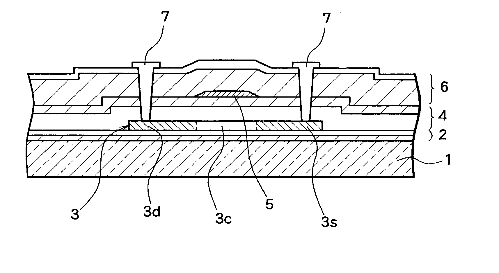
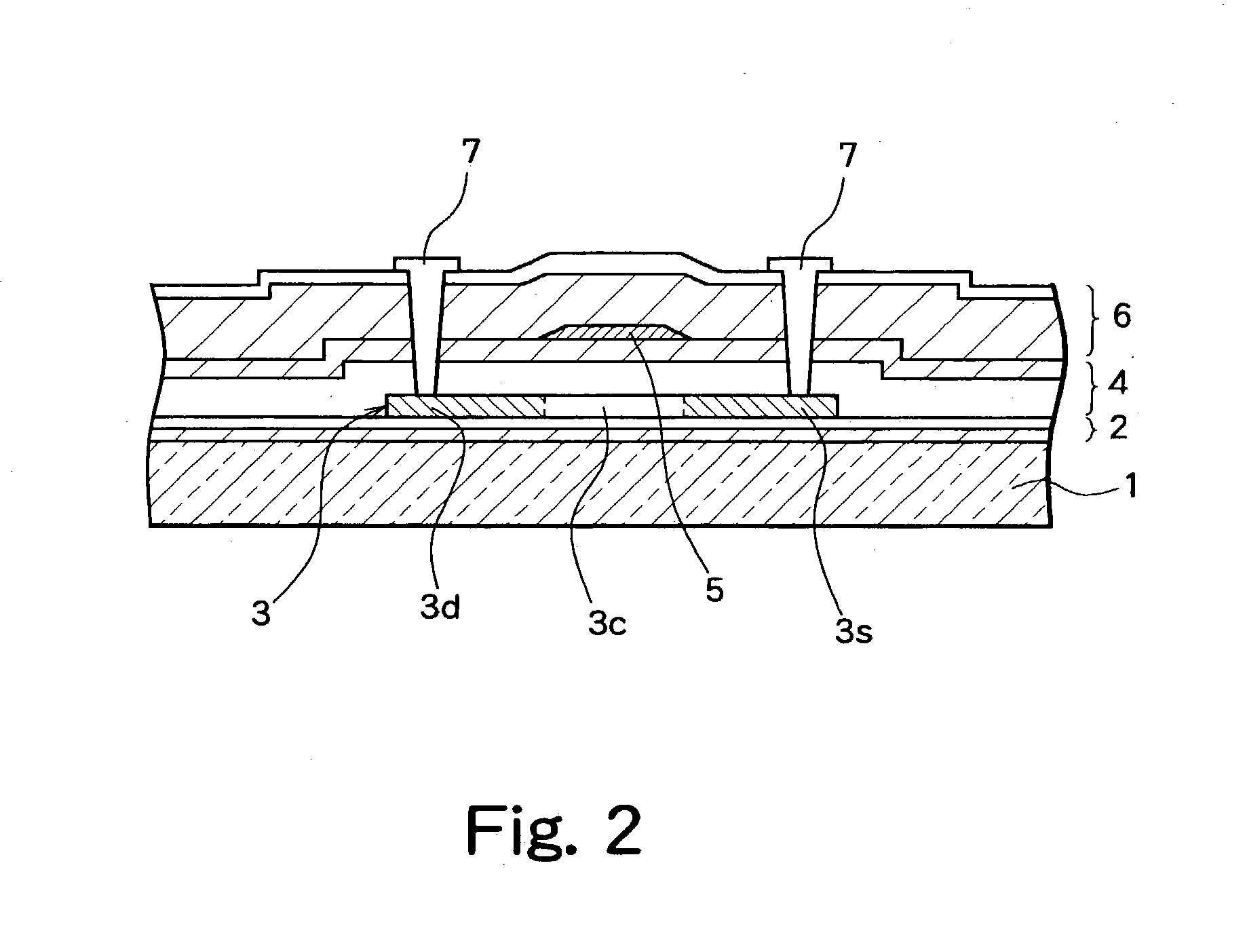
[0040] FIG. 2 shows a cross sectional structure of a TFT according to the embodiment of the present invention. The structure of the TFT according to the embodiment will now be described referring to FIG. 2.

[0041] An insulating film (buffer film) 2 wherein SiN and SiO.sub.2 are layered in that order is formed on a transparent substrate 1 made of glass or the like and a polycrystalline silicon film 3 is formed on the insulating film 2. The polycrystalline silicon film 3 can be formed by various methods such as, for example, a method for directly forming a polycrystalline silicon film through CVD or by a method for forming an amorphous silicon film and then crystallizing the amorphous silicon film to obtain the polycrystalline silicon film. In the latter method, a low temperature process can be employed which allows for the use...


PUM


Abstract

In a thin film transistor having a semiconductor film provided above a substrate, a gate insulating film covering the semiconductor film, a gate electrode formed on the gate insulating film, and an interlayer insulating film covering the gate electrode, the gate electrode has a tapered shape wherein the width becomes wider from the side of the interlayer insulating film towards the gate insulating film. With this structure, the characteristics are stabilized. The electrode having a tapered shape can be formed through a first etching step wherein etching is applied to an electrode material layer to a degree where at least a portion of the electrode material layer remains and a second etching step wherein etching is applied to the electrode material layer while the mask is being ashed.

Description

[0001] 1. Field of the Invention[0002] The present invention relates to a thin film transistor, and, in particular, to a shape for a gate electrode of a thin film transistor.[0003] 2. Description of the Related Art[0004] Thin film transistors (hereinafter abbreviated to "TFT") can be classified based on the position of a gate electrode into a "top gate type", in which the gate electrode is provided above a semiconductor film, and a "bottom gate type", in which the gate electrode is provided below the semiconductor film.[0005] A structure of a top gate TFT in a related art will now be described referring to FIGS. 1A and 1B. FIG. 1A is a plan view of a TFT and FIG. 1B is a cross sectional diagram showing the cross section X-X in FIG. 1A. An insulating film 22 made of SiN (silicon nitride) and / or SiO.sub.2 (silicon oxide) is layered on a transparent substrate 21 made of a material such as glass and a polycrystalline silicon film 23 is formed on the insulating film 22 in an island-like ...

Claims


Application Information

Patent Timeline
Patent Type & Authority Applications(United States)
IPC IPC(8): H01L21/336H01L21/77H01L27/12H01L29/423H01L29/49H01L29/786
CPCH01L29/42384H01L29/4908H01L27/124H01L29/66765H01L29/78603H01L29/66757H01L29/786
Inventor SUZUKI, KOJI
Owner SANYO ELECTRIC CO LTD
Why Eureka
Try Eureka