
Liquid crystal display device, manufacturing method therefor, and electronic apparatus

Active Publication Date: 2004-01-08
BOE TECH GRP CO LTD
View PDF8 Cites 46 Cited by
  • Summary
  • Abstract
  • Description
  • Claims
  • Application Information

AI Technical Summary

Benefits of technology

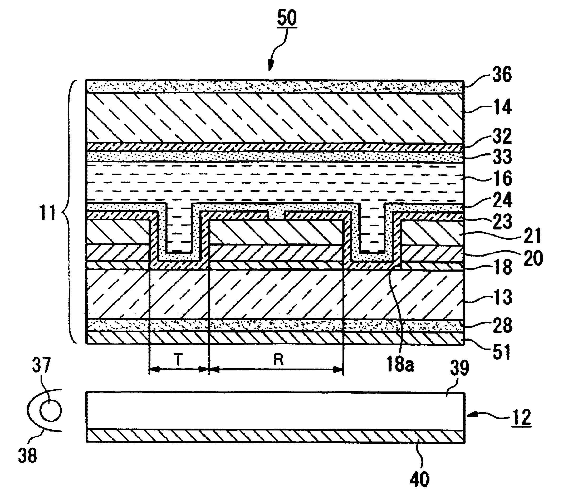
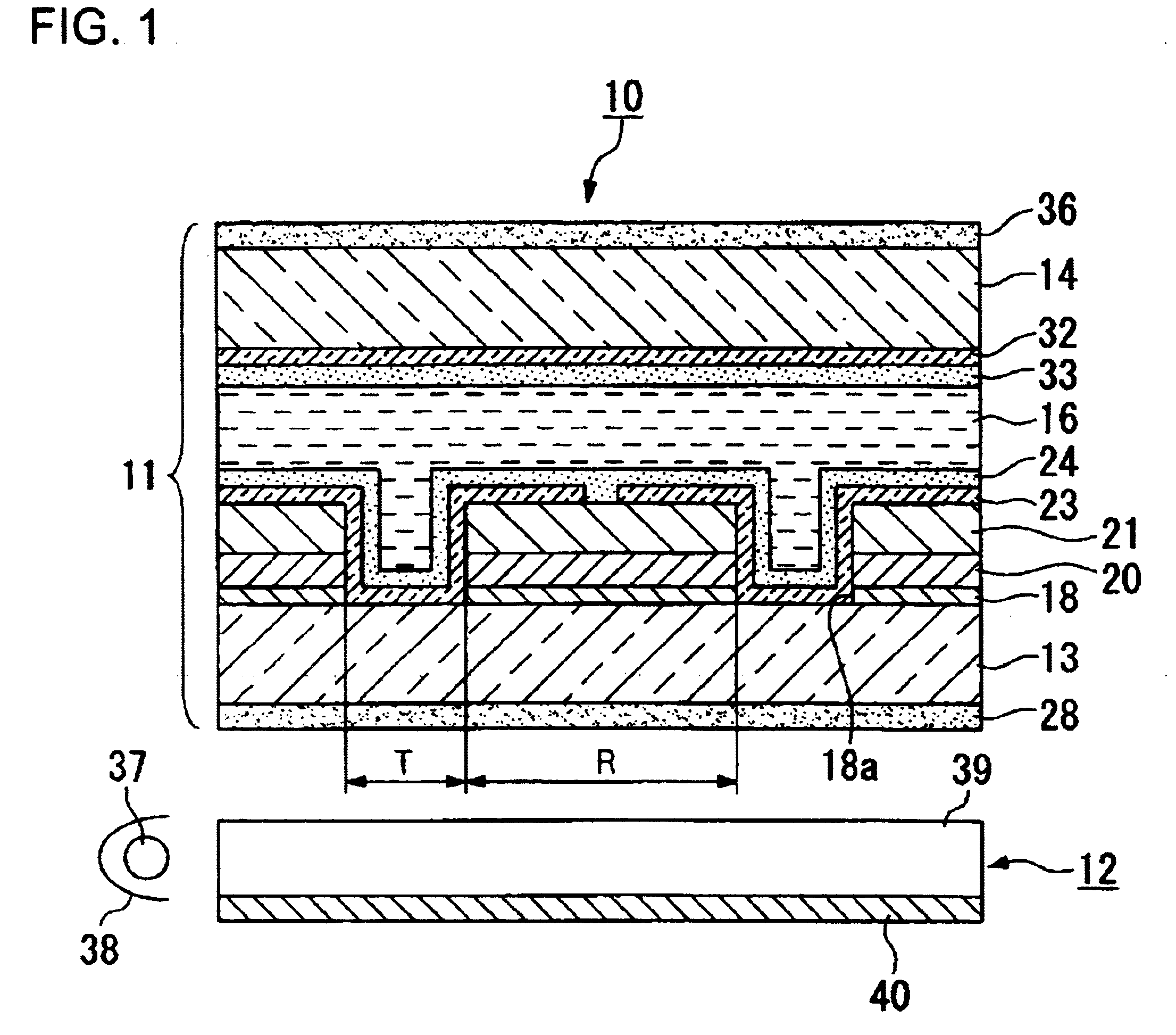
[0042] Any of the methods can relatively easily realize a structure in which the retardation layer is locally formed only in the reflective display region by a conventional photolithography process. For example, the photosensitive resin layer may be formed after the retardation layer is formed, and then patterned by the photolithography process to leave the photosensitive resin layer above the retardation layer. This method can easily realize a structure in which the thickness of the liquid crystal layer in the reflective display region is smaller than that in the transmissive display region.

Problems solved by technology

As described above, the liquid crystal display device 100 shown in FIGS. 7 and 8 is capable of producing a visible display regardless of the presence of external light, but has the problem of insufficient light in a transmissive display in comparison to a reflective display.
Furthermore, the liquid crystal display device shown in FIG. 7 requires pluralities of retardation plates and polarizing plates to be bonded to both outer surfaces of a pair of substrates with a liquid crystal layer sandwiched therebetween, and thus has the problems of complicating the construction, increasing the manufacturing cost, and failing to thin the liquid crystal display device.
Therefore, the problem of darkening the transmissive display due to the absorption of about a half of circularly polarized light by the upper polarizing plate, and the problem of complicating the structure to increase the number of necessary components remain unsolved.
However, it is difficult to actually greatly differentiate the refractive index anisotropy .DELTA.n of the liquid crystal in the transmissive display regions from that in the reflective display region.

Method used


Image

  • Liquid crystal display device, manufacturing method therefor, and electronic apparatus
  • Liquid crystal display device, manufacturing method therefor, and electronic apparatus
  • Liquid crystal display device, manufacturing method therefor, and electronic apparatus

Examples


example 2 example 1 example 2

Transmittance (%) 1.4 2.4 4.3 7.5 Reflectance (%) 30 30 31 31

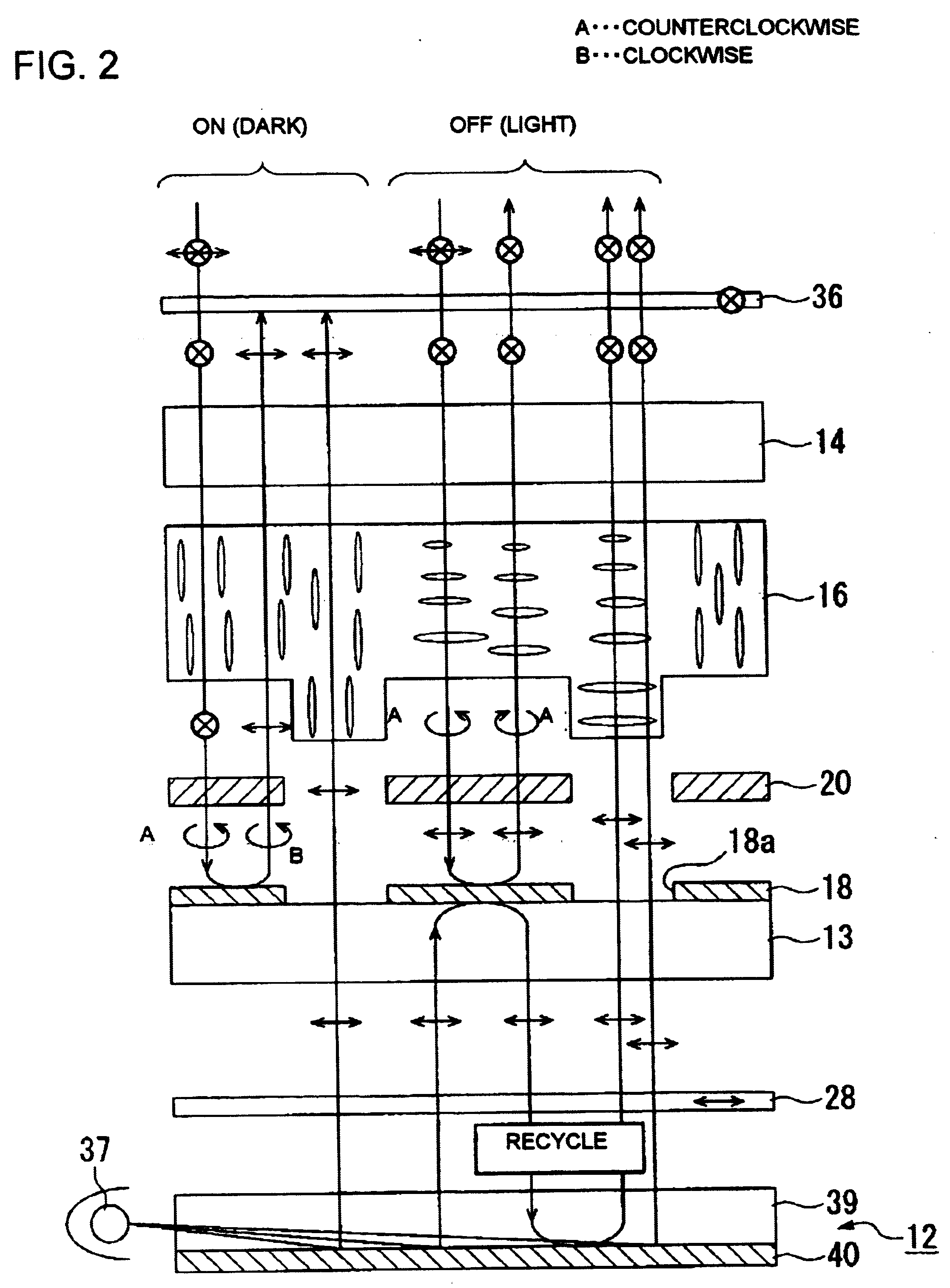
[0135] Table 1 indicates that the four samples have no significant difference in reflectance, and it is thus said that a liquid crystal display device of the present invention exhibits the same level of brightness in a reflective display as a conventional display. On the other hand, in comparison between Comparative Example 1 and Example 1 and between Comparative Example 2 and Example 2, 1.4% of transmittance in Conventional Example 1 increases to 4.3% of transmittance in Example 1, and 2.4% of transmittance in Conventional Example 2 increases to 7.5% of transmittance in Example 2. Namely, in both Examples 1 and 2, the transmittance increases by about 3 times. These results prove that the construction of the present invention has the effect of preventing light passing through a liquid crystal layer from being absorbed by an upper polarizing plate, and the effect of permitting the re-use of light reflected by the back of a ...


PUM


Abstract

An upper polarizing plate 36 is provided on the outer surface of an upper substrate 14, and a lower polarizing plate 28 is provided on the outer surface of a lower substrate 13. Also, a retardation layer 20 having a phase shift of a quarter wavelength, and a protective layer 21 are provided in turn only on reflective display regions R of the inner surface of the lower substrate 13 so that with no voltage applied, the phase shifts of a liquid crystal layer 16 in transmissive display regions T and the reflective display regions R are set to a half wavelength and a quarter wavelength, respectively. Therefore, the present invention provides a transflective liquid crystal display device having improved display brightness in a transmission mode and excellent visibility.

Description

[0001] 1. Field of the Invention[0002] The present invention relates to a liquid crystal display device, a manufacturing method therefor, and an electronic apparatus. Particularly, the present invention relates to a construction of a transflective liquid crystal display device with excellent visibility, which is capable of a sufficiently bright display in both a reflective mode and transmissive mode.[0003] 2. Description of the Related Art[0004] A liquid display device has been proposed for visualizing a display in the light by using external light like in a conventional reflective liquid crystal display device, and visualizing a display in the dark by using an internal light source. The liquid crystal display device uses a display system for both a reflective display and transmissive display so that the display system can be switched to the reflective display or transmissive display according to ambient brightness, thereby permitting a clear display while decreasing power consumpti...

Claims


Application Information

Patent Timeline
IPC IPC(8): G02F1/1333G02B5/30G02F1/1335G02F1/13363G02F1/139
CPCG02F1/133555G02F1/13363G02F2413/09G02F2001/133638G02F2413/01G02F2001/133565G02F1/133565G02F1/133638G02F1/133631
Inventor OZAWA, KINYAHIGA, MASAKATSUIIJIMA, CHIYOAKI
Owner BOE TECH GRP CO LTD
Learn More