Semiconductor device and power source device

a technology of semiconductor devices and power source devices, which is applied in the direction of electric variable regulation, process and machine control, instruments, etc., can solve the problems of environmental problems, increased leakage current, and increased consumption of various types of circuit units, so as to improve power conversion efficiency and be easily changed.

Active Publication Date: 2011-07-14
RENESAS ELECTRONICS CORP
View PDF6 Cites 68 Cited by
  • Summary
  • Abstract
  • Description
  • Claims
  • Application Information

AI Technical Summary

Benefits of technology

[0006]In addition, the environmental problem is of concern in recent years. In various types of circuit units as described above, a power saving design is performed, wherein only necessary minimum circuit blocks are activated in response to a status of the system, and accordingly the range of fluctuation of the consumption current (current range) is expanding. Correspondingly, the POL converter is required to improve the power conversion efficiency in a wide range of current. In the multi-phase type POL converter, the more the number of phases is increased, the higher current can be handled. However, if a light load (various types of circuit units with a small consumption current) is driven under this condition, the power conversion efficiency will decrease. That is, because there is the number of phases which optimizes the power conversion efficiency in response to the consumption current of a load, the POL converter is preferably configured so as to be able to dynamically change the number of phases.
[0012]Then, the present invention has been made in view of the above circumstances and provides a multi-phase power source device capable of easily changing the number of phases and a semiconductor device serving as a constituent element thereof. In addition, the other purposes and the new feature of the present invention will become clear from the description of the present specification and the accompanying drawings.
[0015]Here, the second terminals of the respective semiconductor devices are commonly coupled to each other. Moreover, the fourth terminal of the semiconductor device in a k-th stage is sequentially coupled to the third terminal of the semiconductor device in a (k+1) stage, and the fourth terminal of the semiconductor device in an m-th stage serving as the final stage is fed back to the third terminal of the semiconductor device in the first stage. With such loop connection, the pulse input signal (or pulse output signal) in each semiconductor device differs in a predetermined unit of phase, which makes it possible to realize the multi-phase operation.
[0016]Moreover, the first terminal of each semiconductor device is commonly coupled to an external capacitor, the first switch of the first stage semiconductor device is turned on and the first switches of the other semiconductor devices are turned off. Thereby, a common clock signal is output from the clock signal generation circuit of the first stage semiconductor device toward each semiconductor device. If the number of semiconductor devices commonly coupled to the external capacitor described above (i.e., the number of phases) increases n times, the charge rate and / or the discharge rate automatically increases n times and therefore the frequency of this common clock signal increases n times. By automatically changing the frequency of the common clock signal to n times in response to the number of phases n in this manner, the multi-phase operation at a predetermined switching frequency can be easily realized without depending on the number of phases.
[0017]Furthermore, in the above-described power source device, it is preferable to provide the second switch between the charge and discharge circuit and the first terminal and additionally provide a switch circuit which short-circuits between the third terminal and the fourth terminal and blocks electrical conduction between the pulse signal generation circuit and the fourth terminal, in each semiconductor device. The second switch and the switch circuit are controlled, so that the number of phases can be dynamically changed in response to the consumption current of an external load and an improvement in the power conversion efficiency can be achieved. Note that, for example, the dynamic change of the number of phases, when each semiconductor device performs the switching operation according to the so-called peak current control method, may be automatically performed by monitoring a determination voltage level in determining this peak current.
[0018]To explain briefly the effect acquired by the typical embodiment among the inventions disclosed in the present application, the number of phases can be easily changed in a multi-phase power source device.

Problems solved by technology

Thus, the consumption current of various types of circuit units tends to increase with an increase in the operation frequency, and the leakage current also tends to increase with a decrease in the power source voltage.
In addition, the environmental problem is of concern in recent years.
However, if a light load (various types of circuit units with a small consumption current) is driven under this condition, the power conversion efficiency will decrease.

Method used


Image

  • Semiconductor device and power source device
  • Semiconductor device and power source device
  • Semiconductor device and power source device

Examples


embodiment 1

[0050]>

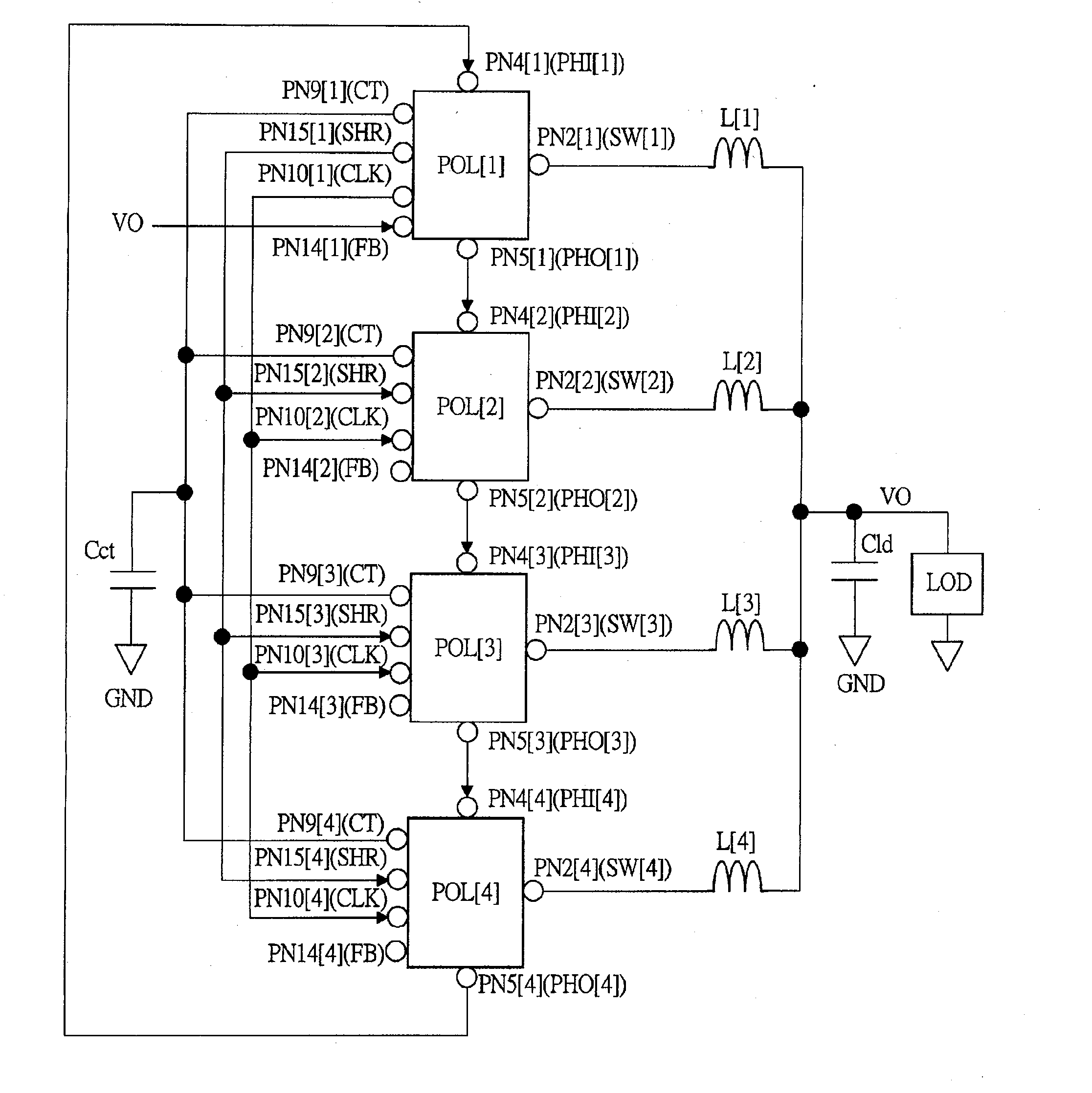
[0051]FIG. 1 is a block diagram showing an example of the outline configuration of a power source device according to Embodiment 1 of the present invention. The power source device shown in FIG. 1 comprises a plurality of (here, four) drive units (semiconductor devices) POL[1]-POL[4] and a plurality of inductors L[1]-L[4], and capacitors Cct, Cld. Each drive unit POL[n] (n=1-4) has an identical internal configuration, and includes seven external terminals PN2[n], PN4[n], PN5[n], PN9[n], PN10[n], PN14[n], and PN15[n]. POL[1] serves as a master drive unit, and POL[2]-POL[4] serve as a slave drive unit, respectively. One ends of L[1]-L[4] are commonly coupled to an output power source node VO, and the other ends of each L[n] are individually coupled to PN2[n], respectively. Cld is provided between VO and a ground power source voltage GND.

[0052]The external terminal PN9[n] of each POL[n] is commonly coupled to one end of the capacitor Cct, through which a clock control signal CT ...

embodiment 2

[0090]>

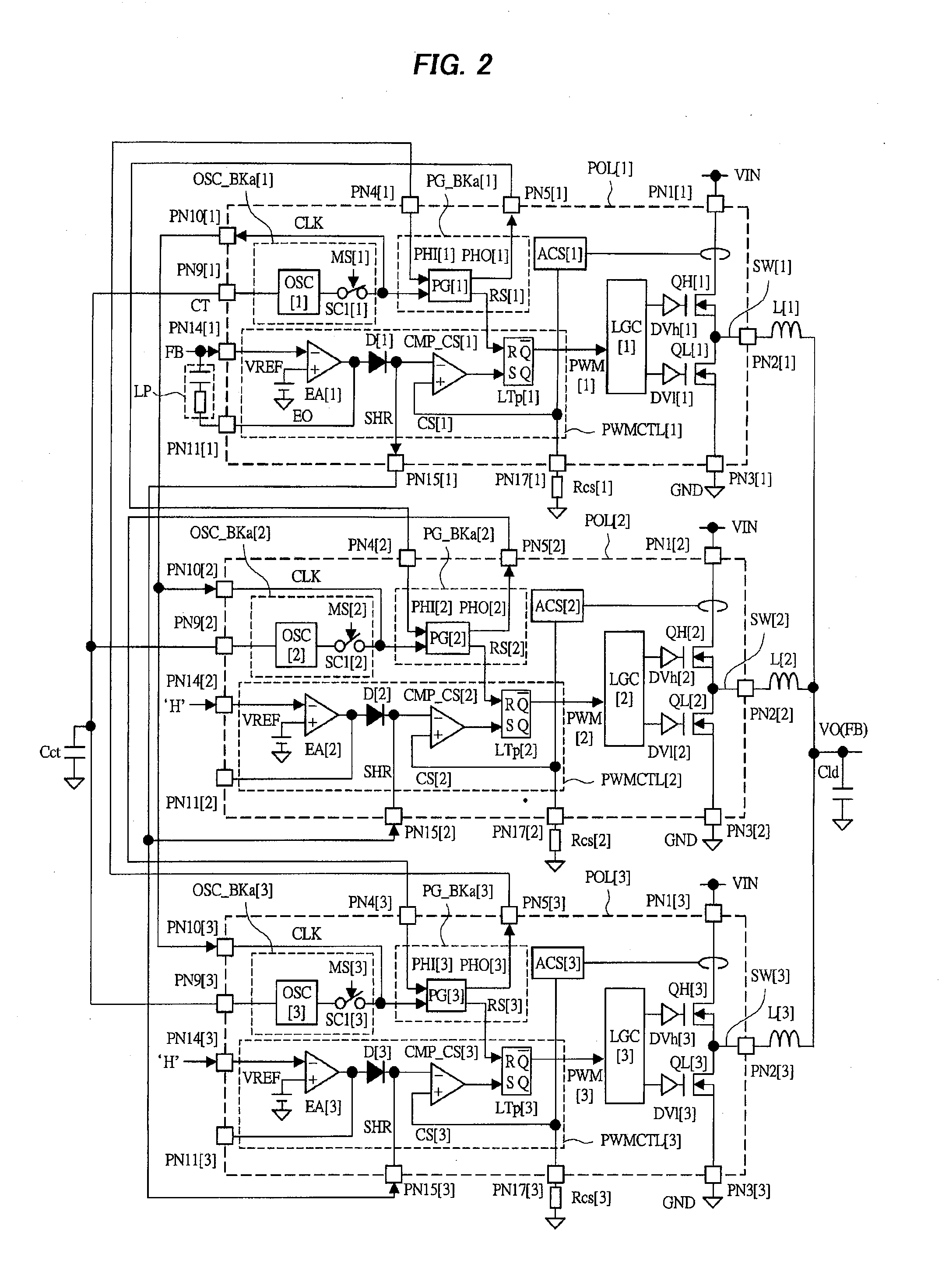
[0091]In Embodiment 2, a configuration example is described in which additional functions are added to the power source device described in FIG. 2 of Embodiment 1. FIG. 8 is a circuit block diagram showing an example of the detailed configuration of the main part in the power source device according to Embodiment 2 of the present invention. The power source device shown in FIG. 8 differs from the power source device of FIG. 2 in terms of the internal configuration of the oscillator circuit blocks OSC_BKb[1]-OSC_BKb[3] and phase signal generation circuit blocks PG_BKb[1]-PG_BKb[3] in each of the drive units POL[1]-POL[3]. Furthermore, each of enable signals EN[1]-EN[3] is input to each of the control logic circuits LGC[1]-LGC[3] in each of POL[1]-POL[3]. The detailed description of the other configuration is omitted because it is the same as that of the power source device of FIG. 2. When EN[n] is in an inactive state, each LGC[n] fixes the transistors QH[n], QL[n] to an off-s...

embodiment 3

[0104]>

[0105]In Embodiment 3, a configuration example is described in which additional functions are added to the power source device described in FIG. 8 of Embodiment 2. FIG. 10 is a circuit block diagram showing an example of the detailed configuration of a main part in a power source device according to Embodiment 3 of the present invention. The power source device shown in FIG. 10 includes external terminals PN11b[n], PN12[n], and an enable detection circuit ENDET[n] added to each drive unit POL[n] (n=1-3), as compared with the power source device of FIG. 8. The detailed description of the other configuration is omitted because it is the same as that of the power source device of FIG. 8.

[0106]>

[0107]FIG. 11 is a circuit diagram showing an example of the detailed configuration of the enable detection circuit ENDET in the power source device of FIG. 10. The enable detection circuit ENDET shown in FIG. 11 includes a comparator circuit CMP_EN receiving the common control signal SHR ...


PUM

PropertyMeasurementUnit
voltageaaaaaaaaaa
charge rateaaaaaaaaaa
voltage levelaaaaaaaaaa

Abstract

A multi-phase power source device capable of easily changing the number of phases is realized. For example, a plurality of drive units POL[1]-POL[4] corresponding to the number of phases are provided, wherein each POL[n] receives a phase input signal PHI[n] serving as a pulse signal, and generates a phase output signal PHO[n] by delaying PHI[n] by a predetermined cycles of a clock signal CLK. PHI[n] and PHO[n] of each POL[n] are coupled in a ring, wherein each POL[n] performs a switching operation with PHI[n] or PHO[n] as a starting point. In this case, each POL[n] charges and discharges a capacitor Cct commonly coupled to each POL[n] with an equal current, and a frequency of CLK is determined based on this charge and discharge rate. That is, if the number of phases increases n times, the frequency of CLK will be automatically controlled to n times.

Description

CROSS-REFERENCE TO RELATED APPLICATION[0001]The disclosure of Japanese Patent Application No. 2010-5956 filed on Jan. 14, 2010 including the specification, drawings and abstract is incorporated herein by reference in its entirety.BACKGROUND OF THE INVENTION[0002]The present invention relates to semiconductor devices and power source devices using the same, and relates to, for example, a technique effectively applied to a switching power source device for converting a high voltage to a low voltage.[0003]For example, Japanese Patent Laid-Open No. 2009-219184 (Patent Document 1) describes a multi-phase power source, wherein a plurality of semiconductor devices corresponding to the respective phases is coupled in a ring (FIG. 1). Moreover, Japanese Patent Laid-Open No. 2006-50891 (Patent Document 2) describes a multi-phase type DC / DC converter device, wherein a plurality of converter control ICs is used to supply an electric power to a load using different phases, respectively (FIG. 1)....

Claims


Application Information

Patent Timeline
Patent Type & Authority Applications(United States)
IPC IPC(8): G05F1/618
CPCH02M3/1584H01L2924/1305H02M2003/1586H01L2924/1306H01L2224/73265H01L2224/49175H01L2224/49171H01L2224/48247H01L2224/48137H01L2224/48091H01L2224/32245H01L24/34H01L2924/13091H01L2924/00014H01L2924/00H01L2924/3011H01L2924/181H01L2224/40095H01L2224/40245H01L24/40H01L2924/14H01L2224/05553H01L2224/73221H01L2224/371H01L2224/84801H01L2224/37147H01L2224/83801H01L2224/8385H01L2224/8485H01L24/37H01L2224/05554H02M3/1586H01L24/84H01L2924/00012
Inventor NAGASAWA, TOSHIO
Owner RENESAS ELECTRONICS CORP
Why Eureka
Try Eureka