Heterojunction field effect transistors using silicon-germanium and silicon-carbon alloys

a technology of hexagonal junction and transistor, which is applied in the direction of transistors, electrical devices, semiconductor devices, etc., can solve the problems of forming defects, and reducing the scalability of cmos transistors at sufficient thickness of ge-containing layers,

Inactive Publication Date: 2004-01-15
INTERNATIONAL RECTIFIER COEP
View PDF6 Cites 88 Cited by
  • Summary
  • Abstract
  • Description
  • Claims
  • Application Information

AI Technical Summary

Problems solved by technology

In the current evolution of semiconductor devices, the limits of traditional scalability of CMOS transistors are rapidly being approached.
Third, the RBL structure must have a sufficiently smooth film for photolithographic processing after strained silicon growth.
In the fabrication of strained silicon growth structures, defects form as a result of a 4% difference in lattice constants between Si and Ge during the growth of Ge-containing layers on silicon.
The associated inherent strain will produce misfit dislocations at sufficient thickness of the Ge-containing layer.
One of the limitations of using SiGe for fabricating RBLs is the requirement of a high germanium content in the relaxed buffer layer (involving a mole fraction of Ge, as mentioned, that is typically in the range of 0.15 to 0.30), in order to achieve sufficient strain and consequent band-bending in the silicon channel.

Method used


Image

  • Heterojunction field effect transistors using silicon-germanium and silicon-carbon alloys
  • Heterojunction field effect transistors using silicon-germanium and silicon-carbon alloys
  • Heterojunction field effect transistors using silicon-germanium and silicon-carbon alloys

Examples


example

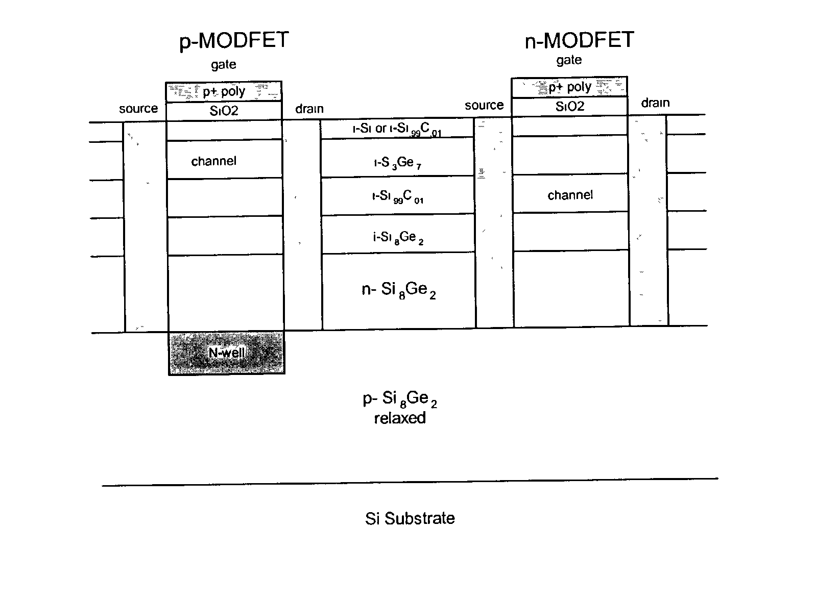
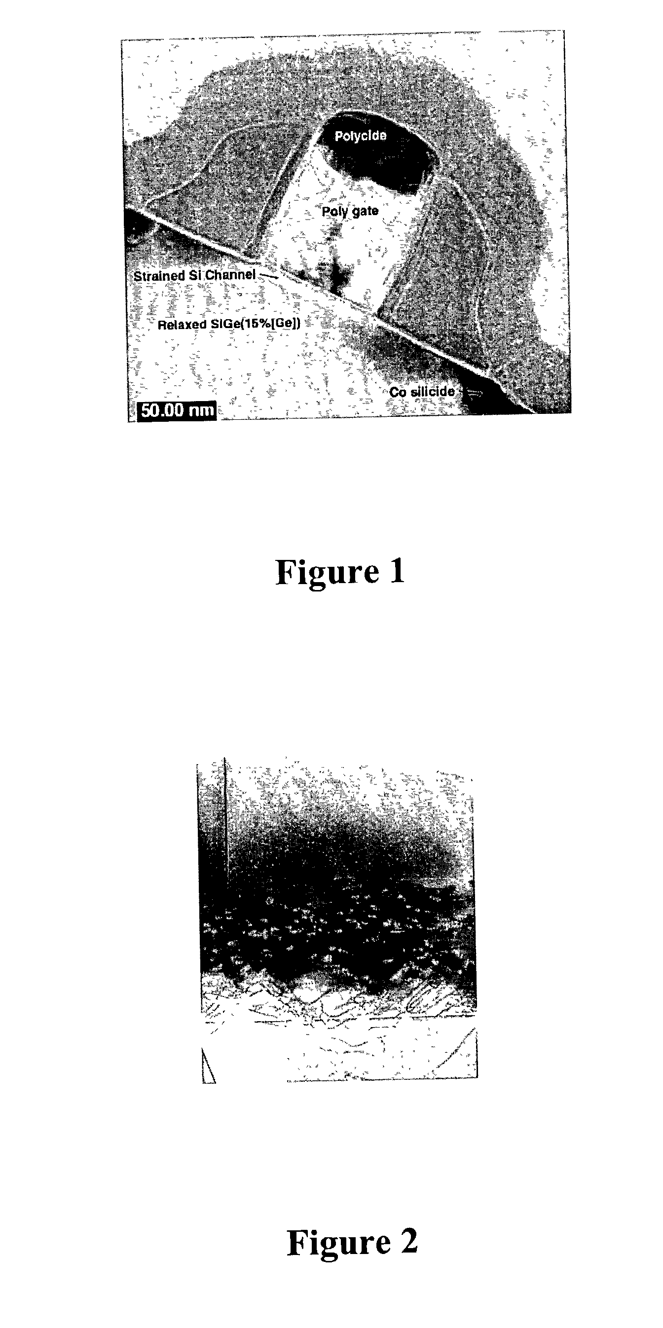
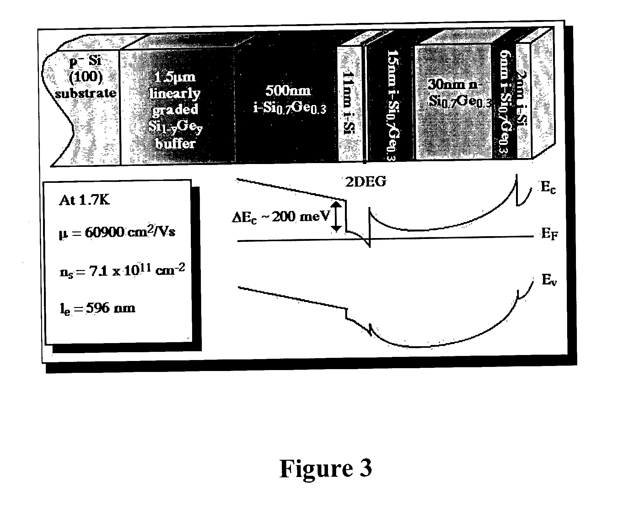
[0061] In an illustrative embodiment, a relaxed buffer layer having a composition of Si.sub.xGe.sub.1-x is grown on a silicon wafer substrate by chemical vapor deposition using dichlorosilane as the silicon precursor and germane as the germanium precursor, at a flow rate to the CVD chamber of 20 standard liters per minute of hydrogen, 200 standard milliliters per minute of dichlorosilane and a flow rate of 10% germane in hydrogen that varies during the growth cycle (0 to 300 standard milliliters per minute). The growth conditions include a temperature of 800.degree. C., and a pressure of 20 torr. Defect density in the near-surface region of the wafer is reduced by compositional grading, which may be combined with thermal annealing cycles. The temperature is reduced to approximately 580.degree. C., and a layer of Si.99C.01 is grown with the following reactor gas flow rates: 100 standard milliliters of silane, 10 standard liters of Hydrogen, and 85 standard milliters of methyl silane....


PUM

PropertyMeasurementUnit
thicknessaaaaaaaaaa
thicknessaaaaaaaaaa
thicknessaaaaaaaaaa

Abstract

Semiconductor devices, e.g., heterojunction field effect transistors, fabricated with silicon-germnanium buffer layer and silicon-carbon channel layer structures. The invention provides a method of reducing threading defect density via reducing germanium content in a SiGe relaxed buffer layer on which a strained silicon channel layer is formed, by forming the strained silicon channel layer of a silicon-carbon alloy, e.g., containing less than about 1.5 atomic % C substitutionally incorporated in the Si lattice of the alloy.

Description

[0001] 1. Field of the Invention[0002] This invention relates to an improvement in so-called "strained silicon" or "band engineered transistor" technology, and encompasses heterojunction field effect transistors fabricated with silicon-germanium and silicon-carbon alloys.[0003] 2. Description of the Related Art[0004] In the current evolution of semiconductor devices, the limits of traditional scalability of CMOS transistors are rapidly being approached. This circumstance in turn has motivated increasing focus on three major groups of new transistors for the future--ultra-thin body silicon-on-insulator (SOI) transistors, band-engineered transistors and double-gate transistors.[0005] Ultra-thin SOI transistors are made in very thin films of silicon about 100-250 Angstroms in thickness.[0006] Band-engineered transistors are based on the approach of using new or modified materials for CMOS devices so that electrons move faster through the structure, such as by use of germanium and induc...

Claims


Application Information

Patent Timeline
Patent Type & Authority Applications(United States)
IPC IPC(8): H01L21/336H01L21/8238H01L27/092H01L29/778H01L31/0328
CPCH01L21/823807H01L29/7786H01L27/0922
Inventor WEBB, DOUGLAS A.WARD, MICHAEL G.
Owner INTERNATIONAL RECTIFIER COEP
Why Eureka
Try Eureka