Base pattern forming material for electrode and wiring material absorption, electrode and wiring forming method, and method of manufacturing image forming apparatus

a technology of base pattern and wiring material, which is applied in the manufacture of photosensitive materials, electric discharge tubes/lamps, instruments, etc., can solve the problems of insufficient uniformity and reproducibility of film thickness, difficult to apply the above-mentioned method, and difficulty in forming a fine circui

Inactive Publication Date: 2004-02-05
CANON KK
View PDF10 Cites 22 Cited by
  • Summary
  • Abstract
  • Description
  • Claims
  • Application Information

AI Technical Summary

Problems solved by technology

However, it is difficult to apply the above-mentioned method (1) to a fine electrode and wiring pattern.
The uniformity and the reproducibility of a film thickness are insufficient even in the case of the above-mentioned method (2).
Therefore, because a resist is attacked or an insulating substrate is eroded, it is difficult to form a fine circuit.
In addition to this, because a large amount of chlorine-based organic solvent is used even in development, there is a problem in that an environmental load is large.
However, because a water-soluble organic metallic compound on an unexposed region is disposed of in the development process, there is a problem in that a cost becomes higher.
However, there is the case where an adhesive property with a substrate is insufficient.
Thus, there is the case where a manufacturing process becomes unstable.
If the compounding ratio of the metallic compound is too large, an electrode and wiring base for a fine pattern is hard to obtain.
On the other hand, if the compounding ratio is too small, an adhesive property of an obtained electrode and wiring pattern is hard to sufficiently improve.

Method used


Image

  • Base pattern forming material for electrode and wiring material absorption, electrode and wiring forming method, and method of manufacturing image forming apparatus
  • Base pattern forming material for electrode and wiring material absorption, electrode and wiring forming method, and method of manufacturing image forming apparatus
  • Base pattern forming material for electrode and wiring material absorption, electrode and wiring forming method, and method of manufacturing image forming apparatus

Examples


embodiment 2

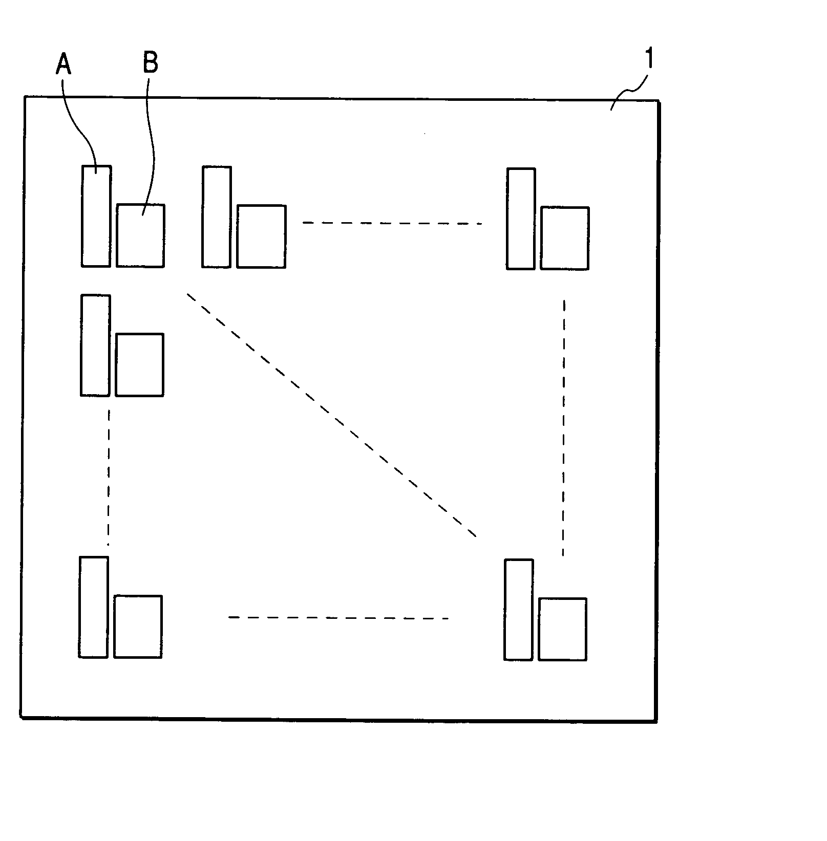
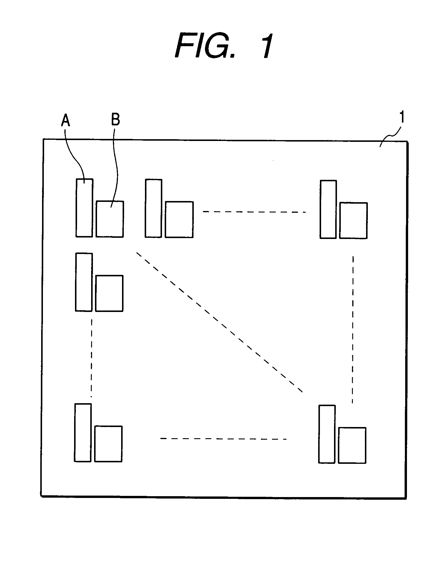
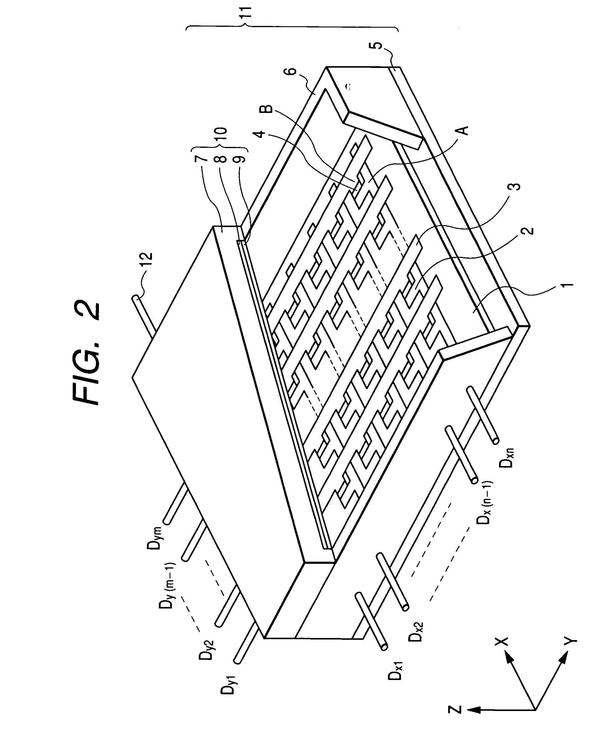
[0081] An image-forming apparatus will be manufactured using the electrode and wiring pattern forming method of the present invention. Hereinafter, a manufacturing order will be described with reference to FIGS. 1 and 2.

[0082] Step 1: A large number of device electrode pairs are formed on a substrate 1 made of glass (300 mm.times.300 mm.times.2.8 mm in thickness) by the same method as in Embodiment 1.

[0083] Each of the device electrode pairs in this embodiment is composed of a device electrode "A" having a width of 60 .mu.m and a length of 480 .mu.m and a device electrode "B" having a width of 120 .mu.m and a length of 200 .mu.m, which are opposed to each other at an interelectrode gap of 20 .mu.m. In addition, pitches of the device electrode pairs are set to 300 .mu.m in the lateral direction and 650 .mu.m in the longitudinal direction. The number of device electrode pairs is 720.times.240 and they are arranged in matrix. A sheet resistance value of a platinum film pattern with 1 c...


PUM

PropertyMeasurementUnit
temperatureaaaaaaaaaa
thicknessaaaaaaaaaa

Abstract

A fine electrode and wiring pattern with a good adhesive property is easily formed using a water-based solution easy to handle and small in environmental load, thereby improving a stability of a manufacturing process of an image-forming apparatus in the case where the water-based solution is used in the manufacturing process. A base pattern is formed using a base pattern forming material for electrode and wiring material absorption which is a water-based solution containing a water-soluble photosensitive resin component and a water-soluble metallic compound including rhodium, bismuth, ruthenium, vanadium, chromium, tin, lead, or silicon. An organic metallic compound is absorbed in the base pattern and then baking is conducted to form electrodes and wirings.

Description

[0001] 1. Field of the Invention[0002] The present invention relates to a base pattern forming material for electrode and wiring material absorption, which is used for forming electrodes and wirings, an electrode and wiring forming method using the base pattern forming material for electrode and wiring material absorption, and a method of manufacturing an image-forming apparatus using the electrode and wiring forming method.[0003] 2. Related Background Art[0004] Up to now, with respect to a method of forming electrodes and wirings on a substrate, there have been known (1) a method of applying a paste containing a conductive material onto a substrate using a screen printing method and conducting drying and baking on the substrate to form electrodes and wirings (Japanese Patent Application Laid-Open No. 8-185818), (2) a method using transfer (Japanese Patent Application Laid-Open No. 8-236017), (3) a method of applying a solution containing metal onto the entire substrate, conducting ...

Claims


Application Information

Patent Timeline
Patent Type & Authority Applications(United States)
IPC IPC(8): G03F7/004G03F7/40H01J9/02H05K3/02H05K3/10
CPCG03F7/0047G03F7/405H01J9/027H05K2203/121H05K3/105H05K2203/0514H05K3/02
Inventor KAGAMI, KAZUHIROTERADA, MASAHIROMORI, SHOSEIFURUSE, TSUYOSHI
Owner CANON KK
Why Eureka
Try Eureka