Light emitting element and manufacturing method for the same

a technology of light emitting elements and manufacturing methods, which is applied in the direction of basic electric elements, electrical equipment, semiconductor devices, etc., can solve the problems of difficult to form such a layer having the continuously changing refractive index on the surface of led, poor extraction efficiency of led chips encapsulated with epoxy resin, and difficult to say that an inherent property

Inactive Publication Date: 2004-02-12
KK TOSHIBA
View PDF2 Cites 63 Cited by
  • Summary
  • Abstract
  • Description
  • Claims
  • Application Information

AI Technical Summary

Problems solved by technology

Accordingly, the extraction efficiency for the LED chip encapsuled with the epoxy resin may become poor.
In fact, it is difficult to form such a layer having the continuously changing refractive index on the surfaces of the LED.
As described above, by tilting and roughening the side surfaces of the LED it is possible to improve the extraction efficiency, however the following new problems arise
Therefore it is difficult to say that an inherent property of the internal quantum efficiency of the light emitting layer is sufficiently exhibited.
(2) Reliability for the LED chip may be decreased due to a nonuniform stress of the molded resin.
Such nonuniform stress exerted on the LED chip causes strain and cracks, as well as a remarkable loss in the long-term reliability of the LED chip.
In addition, excessive stress on the LED chip causes peeling and breakage of the LED chip.
While in rectangular solid LED chips the stresses with the molded resin are balanced out by canceling the stresses applied to opposite side surfaces, since shape symmetry cannot be assured, the stresses generated with the molded resin are extremely difficult to thoroughly eliminate in a trapezoidal LED chip.
Thus, the truncated pyramid LED lamps show a remarkably low survival rate.
While a uniform stress is applied to the side surfaces of the rectangular solid LED chip from the resin, with the truncated pyramid LED chip, stress is applied normal to the tilted side surfaces and therefore, causes an unbalanced stress induced in the upward direction of the LED chip.
Because of the energy of the burn-in current with the unbalanced stress, it is considered that with the truncated pyramid LED chip, penetrating dislocations extend to the light emitting layer so as to decrease the light emitting efficiency.
In addition, although the modified pyramid LED chip has side surfaces that are tilted similar to the truncated pyramid LED chip, the two sets of the opposed side surfaces that are tilted in different directions cancel out the stress of each other so that the unbalanced stress as in the truncated pyramid LED chip is not induced.
Conversely, since linear symmetry is upset and the stress is concentrated in one portion of the truncated pyramid LED chip, many dislocations may be induced.
Such dislocations decrease the brightness of the LED chip and reducing the long term reliability.

Method used


Image

  • Light emitting element and manufacturing method for the same
  • Light emitting element and manufacturing method for the same
  • Light emitting element and manufacturing method for the same

Examples


first embodiment

[0067] The method for manufacturing a modified pyramid LED according to the modified example of the first embodiment is described with referencing FIGS. 10A through 10J.

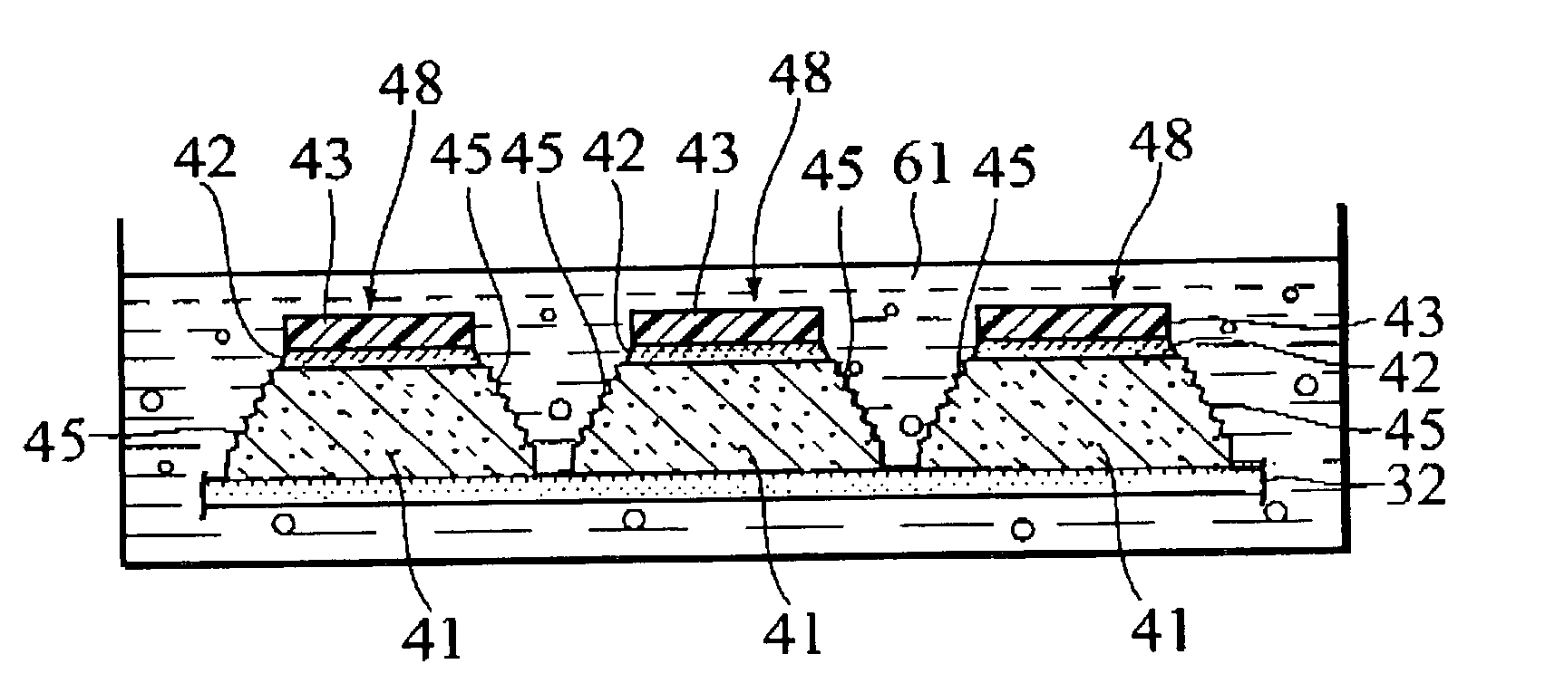
[0068] (a) To begin with, as shown in FIG. 10A, a blade 20 with a V-shaped edge of a point angle of 60 degrees is used on a top surface of an LED wafer 40 affixed upon an acid resistant sheet 32 to perform cutting in one direction and form first cuts 51 (see FIG. 4B).

[0069] (b) Next as shown in FIG. 10B, by immersing in a HCl--H.sub.2O.sub.2 mixed solution 60, damaged layers on the side surface of the first cuts 51, caused by the cutting, is removed and the side surfaces are smoothed. After rinsing with water, as shown in FIG. 10C, the LED wafer 40 is immersed in an HCl solution 61 so that the side surfaces of the first cuts 51 are etched by the HCl solution 61 at 60.degree. C. for 10 minutes. A rough surface 45 is formed on the side surfaces of the first cuts 51.

[0070] (c) Thereafter, rinsing and drying is performed...

second embodiment

[0075] Second Embodiment

[0076] An LED chip 148 according to a second embodiment of the present invention, as shown in FIG. 11, has InGaAlP epitaxial layers including a light emitting layer disposed on a GaP substrate as a base substrate. The base substrate includes the GaP substrate 108 having a p-type conductivity and a p-type GaP layer 107 disposed on the GaP substrate 108. The InGaAlP epitaxial layers includes an n-type current diffusion layer 102, an n-type clad layer 103, an active layer 104, a p-type clad layer 105, and a bonding layer 106. A light emitting layer is the active layer 104 sandwiched between the n-type clad layer 103 and the p-type clad layer 105. The bonding layer 106 of the epitaxial layer is disposed directly on the p-type GaP layer 107 of the base substrate. First and second electrodes 109 and 110 of the LED chip 148 are provided on a bottom surface of the GaP substrate 108 and a top surface of the n-type current diffusion layer 102. The base substrate has ro...


PUM


Abstract

A light emitting element includes: a light emitting layer; a rectangular first principal surface being parallel to the light emitting layer; a rectangular second principal surface opposing to the first principal surface so that the light emitting layer is sandwiched between the first and second principal surfaces; and first through fourth side surfaces of the light emitting element provided with a rough surface, the first through fourth side surfaces connecting between the first principal surface and the second principal surface, respectively so as to define a solid shape.

Description

[0001] This application is based upon and claims the benefit of priority from prior Japanese Patent Application P2002-20185 filed on Jan. 29, 2002 and Japanese Patent Application P2003-16275 filed on Jan. 24, 2003; the entire contents of which are incorporated by reference herein.[0002] 1. Field of the Invention[0003] The present invention relates to a light emitting element having a high level of brightness and a manufacturing method for the same.[0004] 2. Description of the Related Art[0005] An optical power output of a semiconductor light emitting element (LED) is determined by a product of an internal quantum efficiency representing a conversion efficiency of an injection current to photons, and an extraction efficiency for the photons emitted from the semiconductor passing through a molded resin or air. In order to improve the extraction efficiency and increase the optical power output of the LED, many methods have been proposed, such as tilted side surfaces, roughened side and...

Claims


Application Information

Patent Timeline
Patent Type & Authority Applications(United States)
IPC IPC(8): H01L21/301H01L21/306H01L33/16H01L33/22H01L33/30
CPCH01L33/20
Inventor AKAIKE, YASUHIKOWASHIZUKA, SHOICHIKINUGAWA, YOSHIYUKI
Owner KK TOSHIBA
Why Eureka
Try Eureka