

Method of etching a metal layer using a mask, a metallization method for a semiconductor device, a method of etching a metal layer, and an etching gas
- Summary
- Abstract
- Description
- Claims
- Application Information
AI Technical Summary
Benefits of technology
Problems solved by technology
Method used
Image

Examples
Embodiment Construction
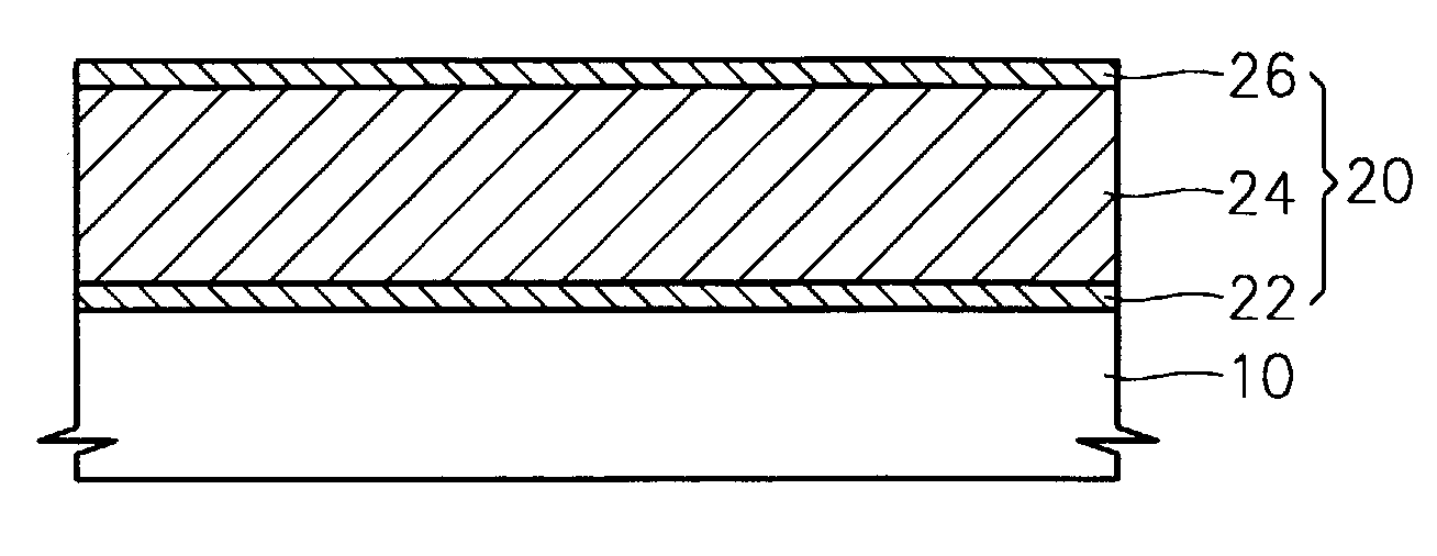
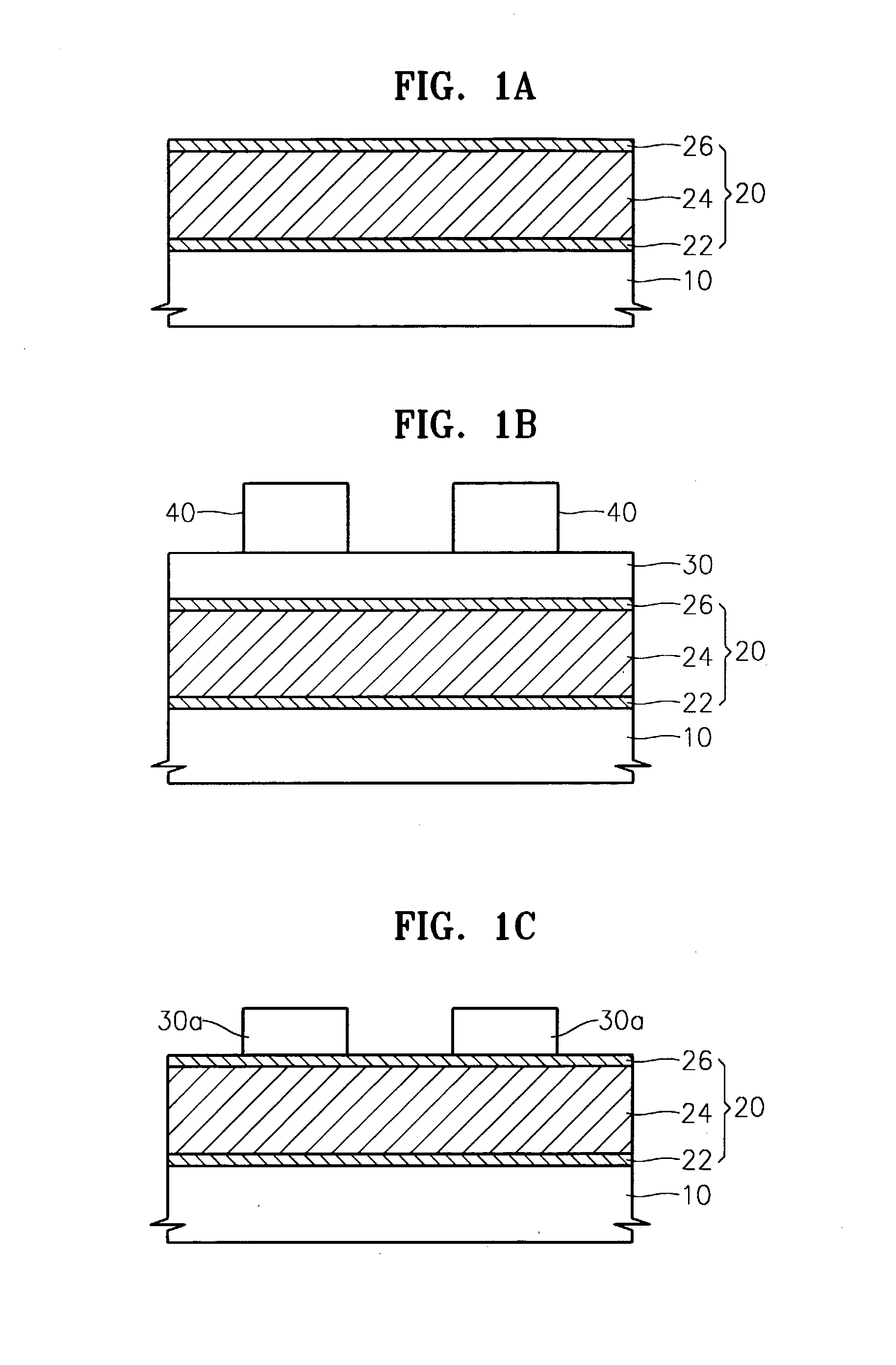
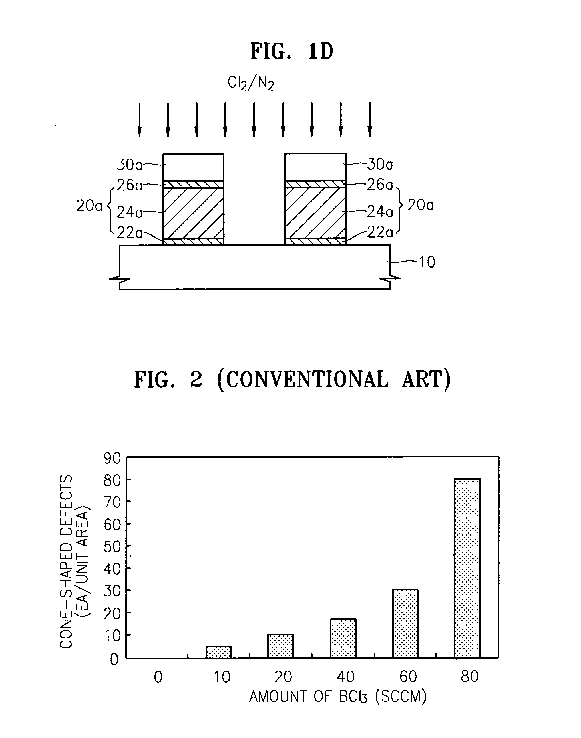
[0020] Exemplary embodiments of the present invention will now be described more fully with reference to the accompanying drawings, in which exemplary embodiments of the invention are shown. This invention may, however, be embodied in many different forms and should not be construed as being limited to the exemplary embodiments set forth herein. Rather, these exemplary embodiments are provided so that this disclosure will be thorough and complete and will fully convey the concept of the invention to those skilled in the art. In the drawings, the thicknesses of layers and regions are exaggerated for clarity. It will also be understood that when a layer is referred to as being "on" another layer or substrate, it may be located directly on the other layer or substrate, or intervening layers may be present. It is to be further understood that when a layer is referred to as being "between" two other layers, it may be positioned such that the two other layers contact the layer, or interve...
PUM
| Property | Measurement | Unit |
|---|---|---|
| Fraction | aaaaa | aaaaa |
| Flow rate | aaaaa | aaaaa |
| Ratio | aaaaa | aaaaa |
Abstract
Description
Claims
Application Information