Multilayered optical information-recording media and process for manufacture thereof

a technology of information-recording media and manufacturing process, applied in the field of multi-layered optical disks, can solve the problems of reducing the precision of film thickness, reducing the productivity of the 2p process relative to that of injection molding, and achieving the effect of both precision and productivity

Inactive Publication Date: 2004-04-01
JVC KENWOOD CORP A CORP OF JAPAN
View PDF6 Cites 0 Cited by
  • Summary
  • Abstract
  • Description
  • Claims
  • Application Information

AI Technical Summary

Benefits of technology

0026] This invention relates to a multilayered optical disk with two or more information-recording surfaces in the thickness direction of a light transmitting substrate, and aims to provide a multilayered optical disk effective in terms of both precision and productivity and a process for the manufacture thereof.

Problems solved by technology

In addition, "the 2P process" is inferior in productivity relative to that of injection molding, requiring as long as 2 minutes per surface for molding a second and subsequent information-recording surfaces.
It may be possible to increase in practice the molding rate of "the 2P process", but that would lead to problems such as reduced film thickness precision, trapping of air bubbles, unsatisfactory suction-removal of the resin overflow, and the like.
That is, manufacture of the above multilayered optical disk by a conventional manufacturing process would be plagued with problems in terms of both precision and productivity.

Method used


Image

  • Multilayered optical information-recording media and process for manufacture thereof
  • Multilayered optical information-recording media and process for manufacture thereof
  • Multilayered optical information-recording media and process for manufacture thereof

Examples


example 1

OF A PROCESS FOR THE MANUFACTURE OF AN OPTICAL DISK

[0053] Next, the process for the manufacture of the above optical disk 1 is described.

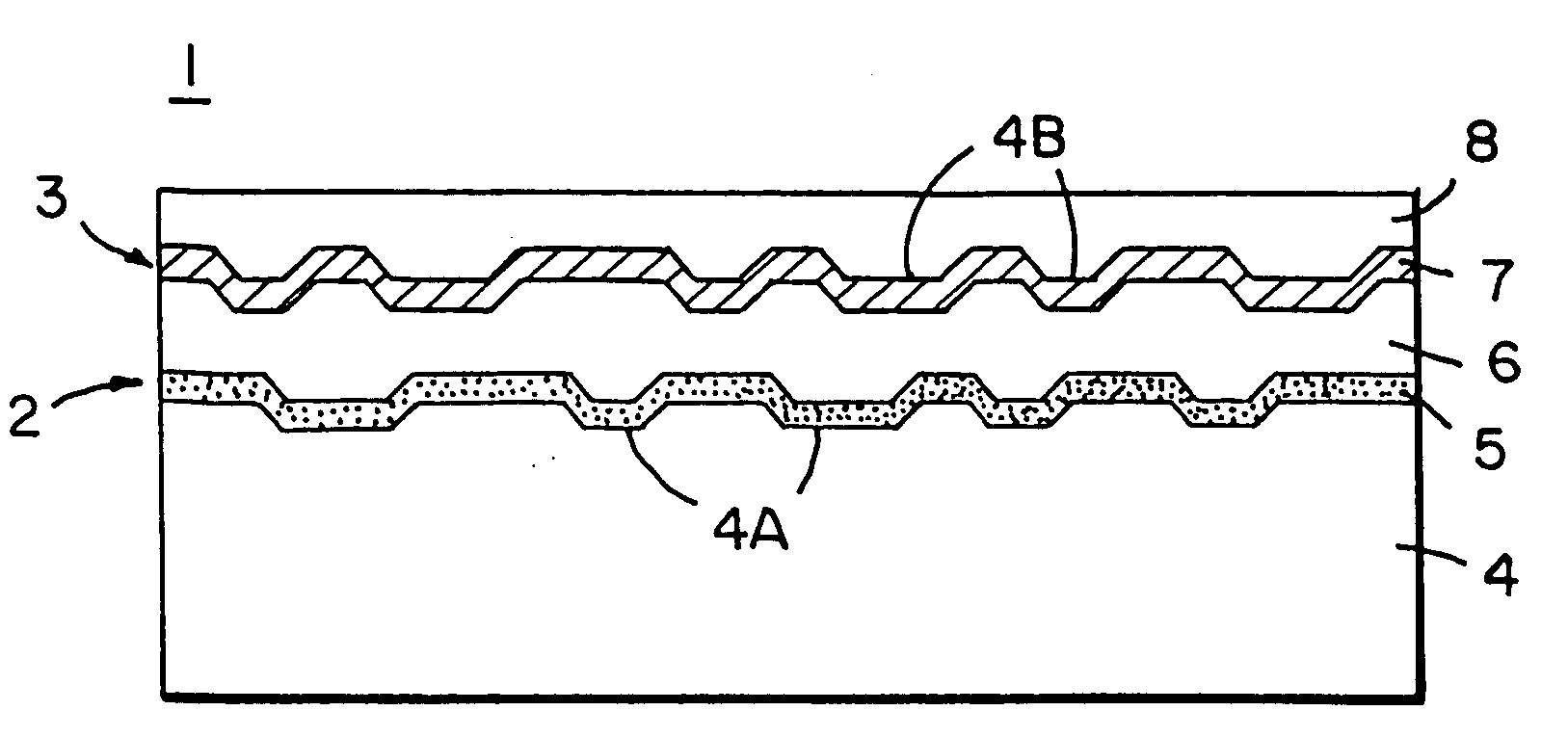
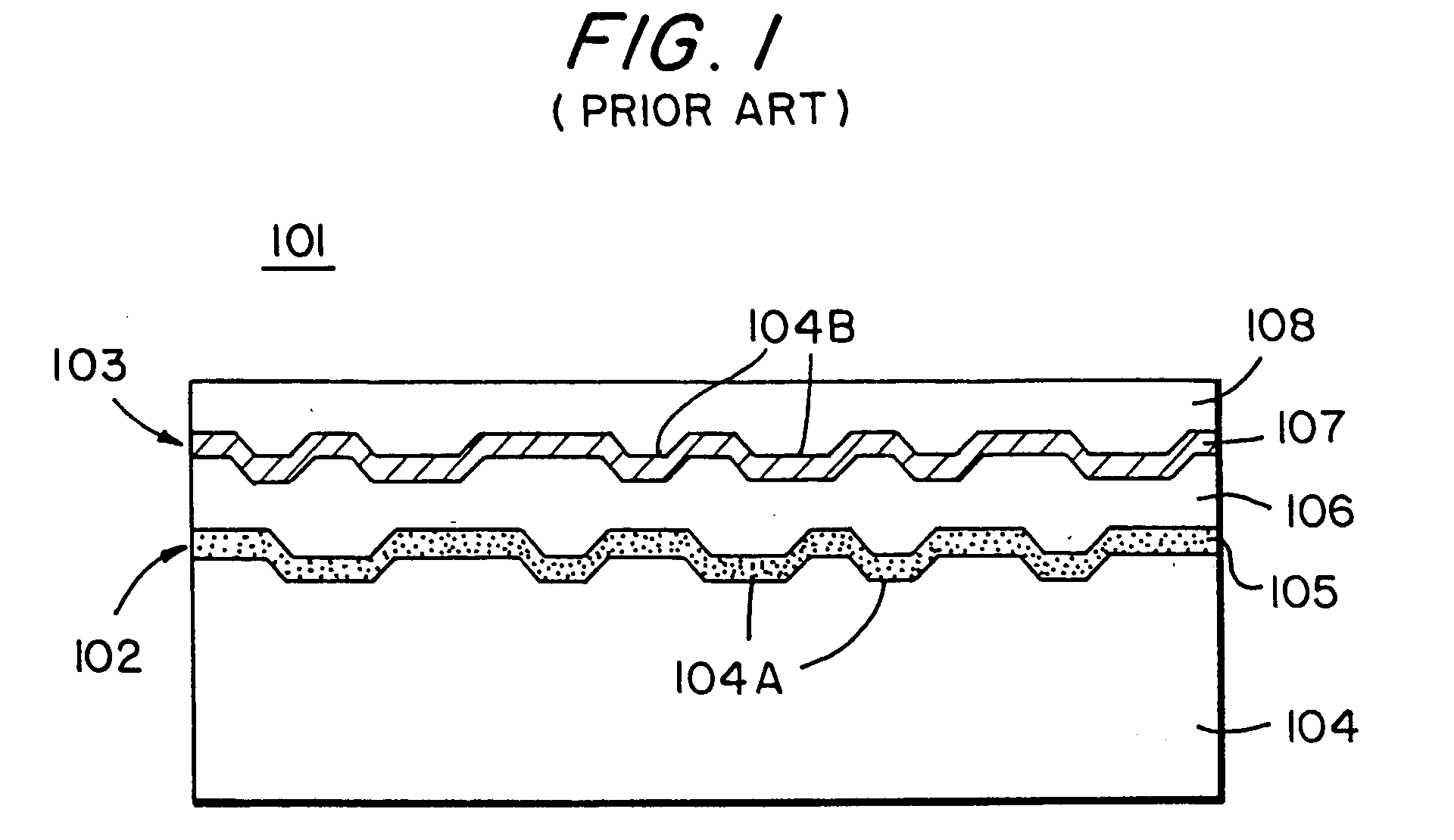
[0054] FIG. 4 is a drawing illustrating an embodiment of the process for the manufacture of the optical disk of this invention shown in FIG. 3. For simplicity, the description is made of a two-layered disk.

[0055] As illustrated in FIG. 4(A), an optical disk substrate 4 with pits 4A on the surface thereof is molded, for example, by injection molding using a stamper (not illustrated) with a pattern negative to pits A of the first information-recording surface.

[0056] Next, as illustrated in FIG. 4(B), a first reflecting layer 5 is formed on the surface on which are formed pits 4A of substrate 4 by a film-forming method such as sputtering, vacuum vapor depositing, spin coating, or the like. As described above, the first reflecting film is a reflecting layer having a certain degree of light transmittance.

[0057] Then, a second information-recording surfa...

example 2

OF A PROCESS FOR THE MANUFACTURE OF AN OPTICAL DISK

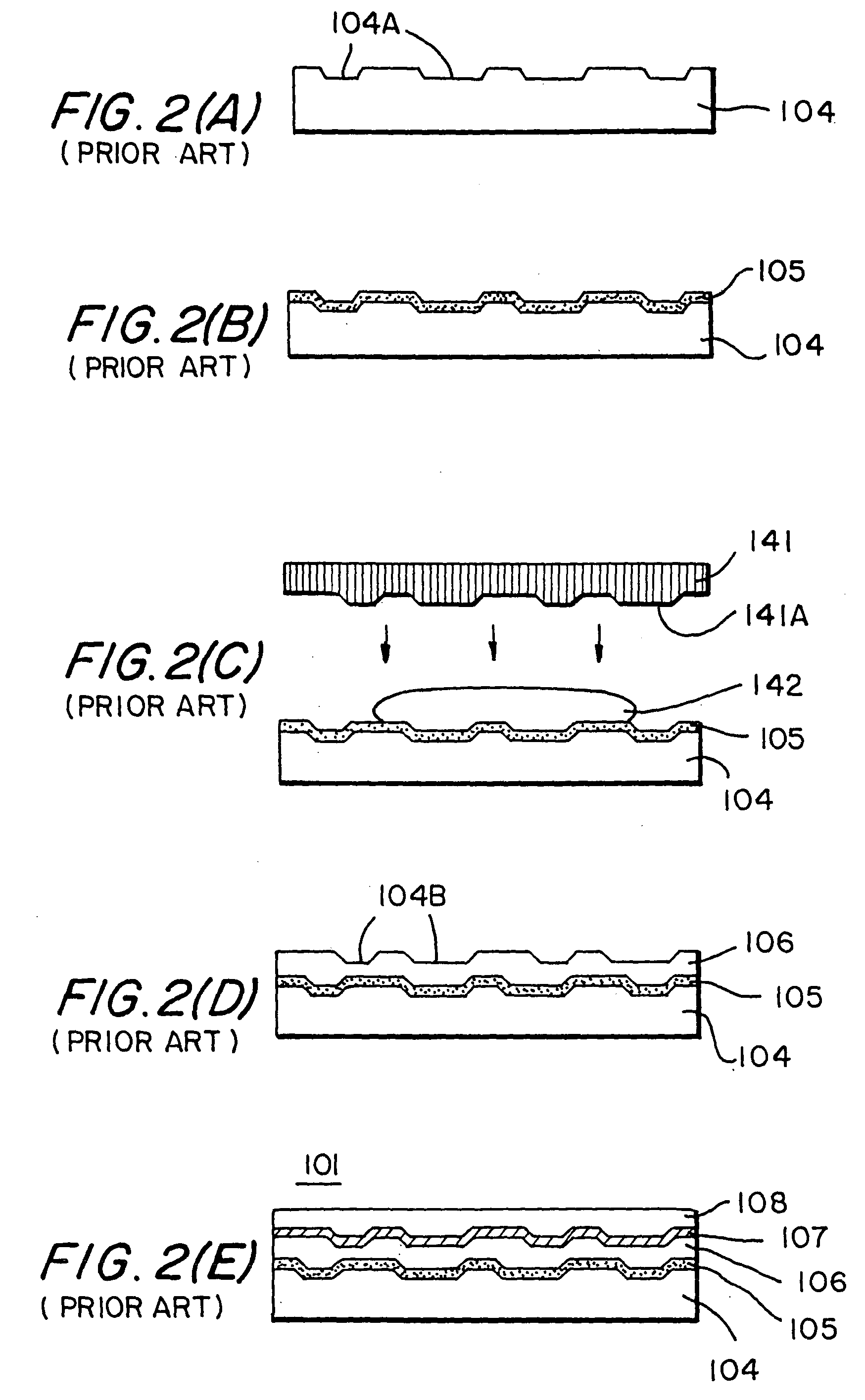
[0071] A reflecting film may be precoated to one surface of the above thermoplastic resin sheet in the above process for the manufacture of optical disks 1 and 11, which are shown in FIG. 3 and FIG. 6, respectively.

[0072] As illustrated in FIG. 7(A), a reflecting film 38 is precoated to one surface of the thermoplastic resin sheet 37, and the sheet is placed to position the side having the reflecting film 38 formed thereon to face the stamper 36. The reflecting film 38 coated to the thermoplastic resin sheet 37 becomes upon molding a second reflecting layer 7. When the thermoplastic resin sheet 37 having the reflecting layer coated thereto is processed with heat and pressure as described above and rapidly cooled, the pattern of crenulated pits 36A of the stamper 36 is transferred to the surface of the thermoplastic resin sheet 37 having the reflecting film 38 formed thereon. Cutting out the molded thermoplastic resin 37 along the ou...

experiment example 1

[0076] Two pieces of nickel stamper with digitized image signals inscribed thereinto in a 0.84 .mu.m track pitch and a pit length 0.45 .mu.m or longer were used. One of them was used to produce a first information-recording surface by injection molding polycarbonate, thereby forming a substrate 4 with a 120 mm diameter and a 1.2 mm thickness having pits 4A of the first information-recording surface formed thereon. A high transmitting first reflecting layer 5 was formed on the surface of the substrate 4 having the formed pits.

[0077] Then, the substrate was mounted on mold 33 of the above molding device 31 not equipped with either the above vacuum chamber 32 or vacuum pump 35. The mold 33 was heated to 70 .degree. C. Acrylic resin (PMMA) sheet (thermoplastic sheet) 37 with a double pass birefringence in the plane of not more than +15 nm was used, which was available as a 15 cm wide and 500 m length cut roll with a film thickness of 50 .mu.m (film thickness variation range .+-.1 .mu.m)...


PUM

PropertyMeasurementUnit
thicknessaaaaaaaaaa
thicknessaaaaaaaaaa
thicknessaaaaaaaaaa

Abstract

This invention provides an optical disk effective in both precision and productivity, and to a process for the manufacture thereof. The optical disk allows reading of the information recorded on each information-recording surface of the two or more information-recording surfaces by varying the focal position of a playback laser beam incident on and passing through said light transmitting substrate; and the optical disk is provided with a transparent layer that is laminated onto the light transmitting substrate and is constituted of a thermoplastic resin sheet of uniform thickness and the transparent layer has an information-recording surface other than the surface of said light transmitting substrate formed thereon.

Description

[0001] 1. Field of the Invention[0002] This invention relates to a mutilayered optical information-recording medium (hereafter, optical disk) that has two or more information-recording surfaces in the thickness direction of a light transmitting substrate and a process for the manufacture thereof.[0003] 2. Description of the Prior Art[0004] Optical disks which record optically readable information and allow reading of the recorded information using a laser beam spot have heretofore been available. Optical disks including compact disks (CDs) and CD-ROMs have become widespread in use, particularly over the recent years.[0005] CD-ROMs recently have come to be used not only in computers but also in multimedia game CD-ROMs and are increasingly replacing magnetic disks (floppy disks) and ROM cartridges both in computer and game applications. Furthermore, a high density CD version called the DVD (digital videodisk) is about to enter the field of movies and multimedia.[0006] Recently proposa...

Claims


Application Information

Patent Timeline
Patent Type & Authority Applications(United States)
IPC IPC(8): G11B7/24G11B7/26
CPCG11B7/24G11B7/2534G11B7/2542G11B7/256G11B7/2575Y10T156/1039G11B7/2595G11B7/263Y10T156/108Y10T156/1023G11B7/2585
Inventor KONDO, TETSUYANISHIZAWA, AKIRA
Owner JVC KENWOOD CORP A CORP OF JAPAN
Why Eureka
Try Eureka