

Method of disposing spacer and method of manufacturing electro-optic device
- Summary
- Abstract
- Description
- Claims
- Application Information
AI Technical Summary
Benefits of technology
Problems solved by technology
Method used
Image

Examples
exemplary embodiment 1
[0035] [Exemplary Embodiment 1]
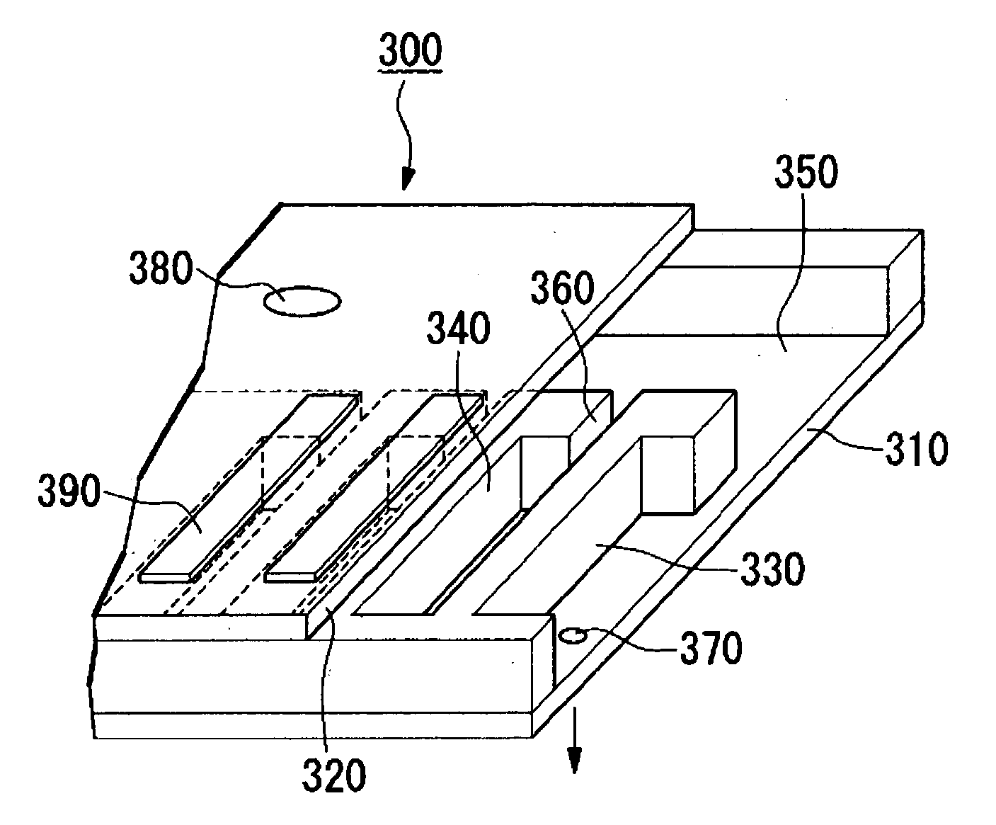
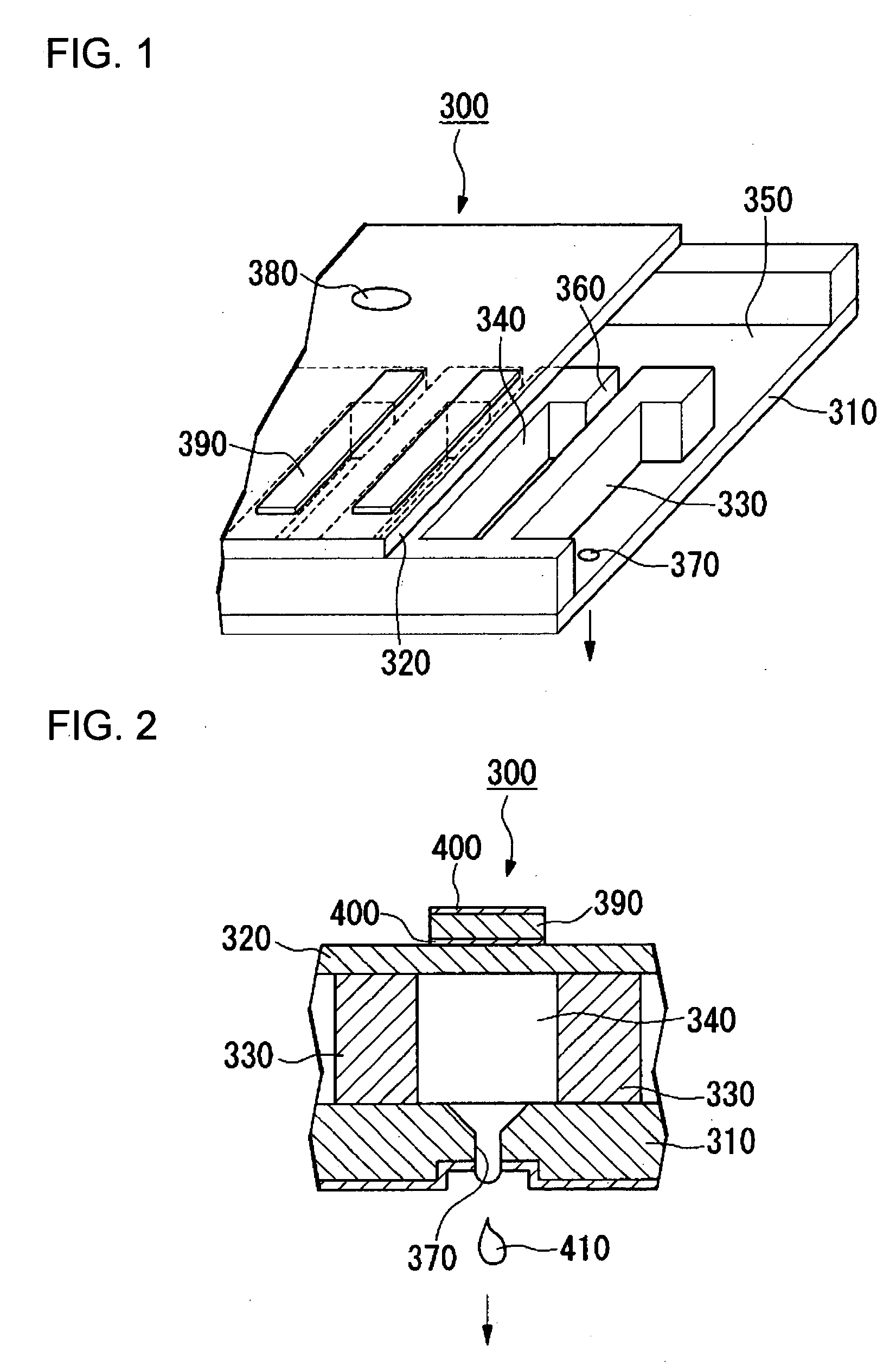
[0036] The spacers have been disposed using the ink jet unit provided with an ink jet nozzle 300 shown in FIGS. 1 and 2.
[0037] In this exemplary embodiment, an examination was made for the conditions of discharge from the nozzle 300, the forms of droplets after they had reached the substrate, etc., when spacers dispersed in the solvents listed in Table 1 were discharged. In this examination, the diameter of the nozzle was 20 .mu.m, the amount of a droplet discharged in one discharge operation was about 20 pico liters, and the distance between the nozzle 300 and a substrate (lower substrate 102) was 800 .mu.m. As for the polypropylene glycol, samples having different mean molecular weights were used to examine the relation between the viscosity and the discharge condition, but we did not make any examination for the spacers' arrangement conditions. In addition, the substrates were heated for three minutes at 150.degree. C. after the discharge, and then ...
exemplary embodiment 2
[0044] [Exemplary Embodiment 2]
[0045] Spacers have been disposed using the ink jet unit provided with an ink jet nozzle 300 shown in FIGS. 1 and 2.
[0046] In this exemplary embodiment, an examination was made for the conditions of discharge from the nozzle 300, the forms of droplets after they had reached the substrate, etc., when spacers dispersed in the solvents listed in Table 1 were discharged. In this examination, the diameter of the nozzle was 20 .mu.m, the amount of a droplet discharged in one discharge operation was about 20 pico liters, and the distance between the nozzle 300 and a substrate (lower substrate 102) was 800 .mu.m. As for the polypropylene glycol, samples having different mean molecular weights were used to examine the relation between the viscosity and the discharge condition, but an examination for the spacers' arrangement conditions was not made. In addition, the substrates were dried for three minutes at 60.degree. C. after the discharge, and then examined f...
exemplary embodiment 3
[0053] [Exemplary Embodiment 3]
[0054] Spacers have been disposed using the ink jet unit provided with an ink jet nozzle 300 shown in FIGS. 1 and 2.
[0055] In this exemplary embodiment, an examination was made for the conditions of discharge from the nozzle 300, the forms of droplets after they had reached the substrate, etc., when spacers dispersed in the solvents listed in Table 1 were discharged. In this examination, the diameter of the nozzle was 12 .mu.m, the amount of a droplet discharged in one discharge operation was about 4 pico liters, and the distance between the nozzle 300 and a substrate (lower substrate 102) was 800 .mu.m. In addition, the substrates were dried for three minutes at 150.degree. C. after the discharge, and then examined for the spacers' arrangement conditions after the evaporation of the solvents. As for the polypropylene glycol, samples having different mean molecular weights were used to examine the relation between the viscosity and the discharge condit...
PUM
| Property | Measurement | Unit |
|---|---|---|
| Pressure | aaaaa | aaaaa |
| Pressure | aaaaa | aaaaa |
| Angle | aaaaa | aaaaa |
Abstract
Description
Claims
Application Information