
Compaction scheme in NVM

a technology of nvm and composite scheme, which is applied in the direction of static storage, digital storage, instruments, etc., can solve the problems of programming failure, undesirable column leakage current, and most troublesome variable in erased threshold voltages

Inactive Publication Date: 2004-06-17
PROGRESSIVE SEMICON SOLUTIONS
View PDF6 Cites 85 Cited by
  • Summary
  • Abstract
  • Description
  • Claims
  • Application Information

AI Technical Summary

Problems solved by technology

As might be expected, the variance in erased threshold voltages is most troublesome at the extremities of the distribution.
Conversely, an NVM cell with a low erased V.sub.T may remain somewhat conductive, even though unselected, thereby contributing to undesirable column leakage current.
Furthermore, an over-erased NVM will present an excessive current load during programming, which may in fact lead to programming failures.
However, soft programming is deemed a less than optimal response to erasure anomalies in that it broadens the distribution in erased V.sub.T.
In addition, this approach requires bit-by-bit selection, which significantly slows the erase time.
If READ voltage is required to be high, charge pumping introduces additional delay, thereby degrading read access speed.
In large part, the remedial measures entertained to date are deficient in their common failure to directly address the source of the difficulties relating to erased cell threshold voltage.

Method used


Image

  • Compaction scheme in NVM
  • Compaction scheme in NVM
  • Compaction scheme in NVM

Examples


Embodiment Construction

(s)

[0023] For a thorough understanding of the subject Compaction Scheme in NVM, reference is made to the following Detailed Description, which includes the appended Claims, in conjunction with the above-described Drawings.

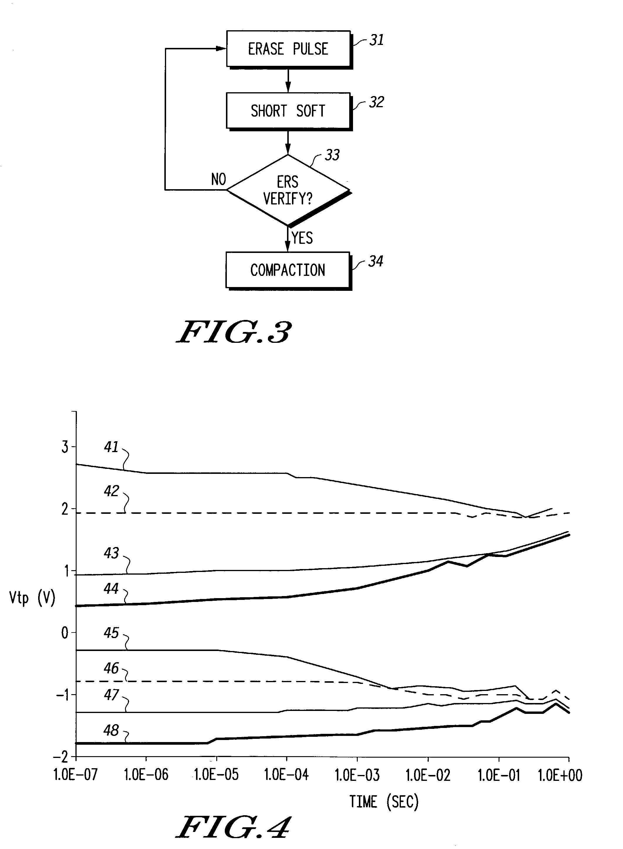
[0024] In a manner that will be made imminently clear below, the subject invention subsists, in one form, in a method of erasing an NVM cell, or a number of NVM cells, in a manner so that the erased V.sub.T of the cell(s) more closely conforms to a target erased V.sub.T. Convergence of the distribution of erased threshold voltages (i.e., compaction) extenuates operational difficulties that derive both from undesirably high erased V.sub.T (falsely read data) and undesirably low erased V.sub.T (column leakage current).

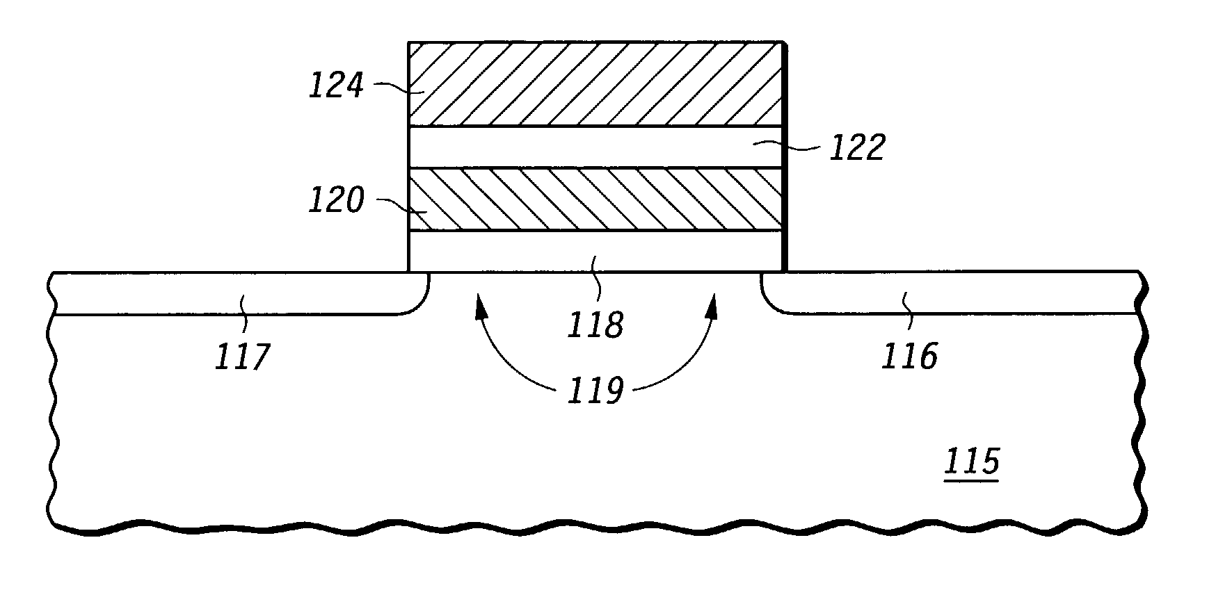
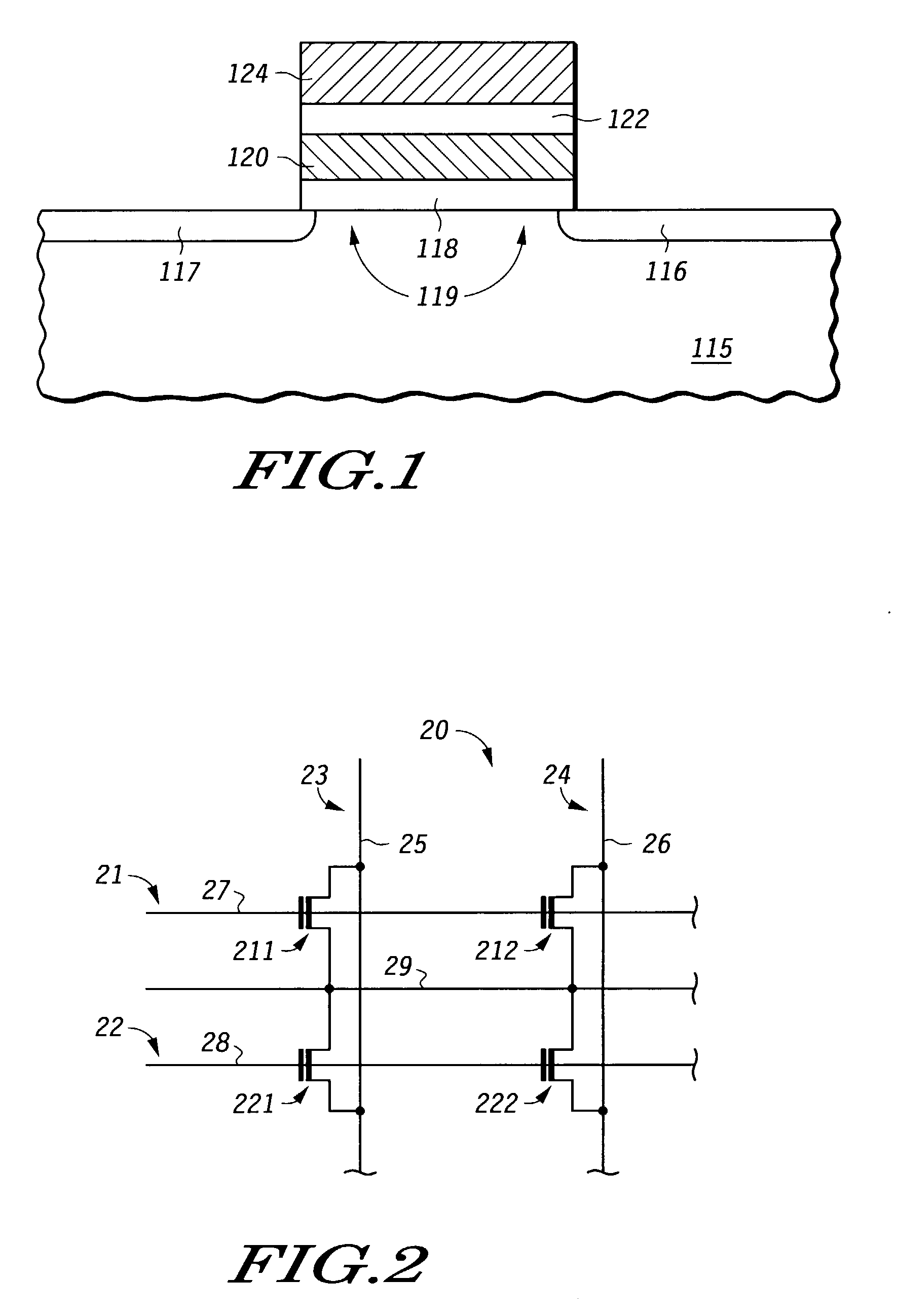
[0025] Directing attention to FIG. 1, depicted there is an NVM cell predicated on a particular thin-film storage construction. The NVM cell depicted in FIG. 1 relies on a thin film of, for example, silicon nitride for charge storage and data retention. ...


PUM


Abstract

A method of erasing a semiconductor nonvolatile memory (NVM) so as to compact the distribution of cell erased threshold voltages within a restricted range around a target erased threshold voltage. Erase pulses are applied to NVM cells until a determination is made by, for example, sensing total column source current that adequate erasure has been realized. An optional soft program signal may be applied subsequent to each erase pulse in order to impede over-erasure. Once erasure has been verified, the distribution of erased threshold voltages is compacted by sustaining, for a predetermined length of time, the simultaneous application of a gate voltage that is equal to the target erased threshold voltage and a highly positive drain voltage.

Description

[0001] 1. Field of the Invention[0002] The subject invention relates generally to the operation of a semiconductor nonvolatile memory (NVM) and, in particular, to a method of erasing an NVM so as to more tightly control the value of the threshold voltage imparted to the NVM cell as a result of an erase operation.[0003] 2. Related Art[0004] Semiconductor NVMs, and particularly electrically erasable, programmable read-only memories (EEPROMs), exhibit widespread applicability in a range of electronic equipments from computers, to telecommunications hardware, to consumer appliances. In general, EEPROMs serve a niche in the NVM space as a mechanism for storing firmware and data that must be refreshed periodically in situ. The EEPROM's precursor, the EPROM, can be erased only through UV irradiation and therefore requires removal from its target system prior to erasure. The flash EEPROM may be regarded as a specifically configured EEPROM that may be erased only on a global or sector-by-sec...

Claims


Application Information

Patent Timeline
IPC IPC(8): G11C16/14G11C16/34
CPCG11C16/3468G11C16/14
Inventor LI, CHI NAN BRIAN
Owner PROGRESSIVE SEMICON SOLUTIONS
Learn More