CMP slurry for semiconductor device, and method for manufacturing semiconductor device using the same

a technology of chemical mechanical polishing and semiconductor devices, which is applied in the direction of manufacturing tools, other chemical processes, chemistry apparatus and processes, etc., can solve the problems of reducing the size of the device, forming a lot of scratches 21 in the polished region, and affecting so as to improve the yield of the semiconductor device and prevent failure. , the effect of high affinity

Inactive Publication Date: 2004-07-01
SK HYNIX INC
View PDF9 Cites 41 Cited by
  • Summary
  • Abstract
  • Description
  • Claims
  • Application Information

AI Technical Summary

Benefits of technology

[0033] A CMP slurry composition including an additive having high affinity to a nitride film is disclosed herein to improve a yield of a semiconductor device by preventing failure due to exposure of the word line when the polysilicon plug is formed via a CMP process, and to prevent scratches on the semiconductor substrate when an STI type device isolation film is formed.

Problems solved by technology

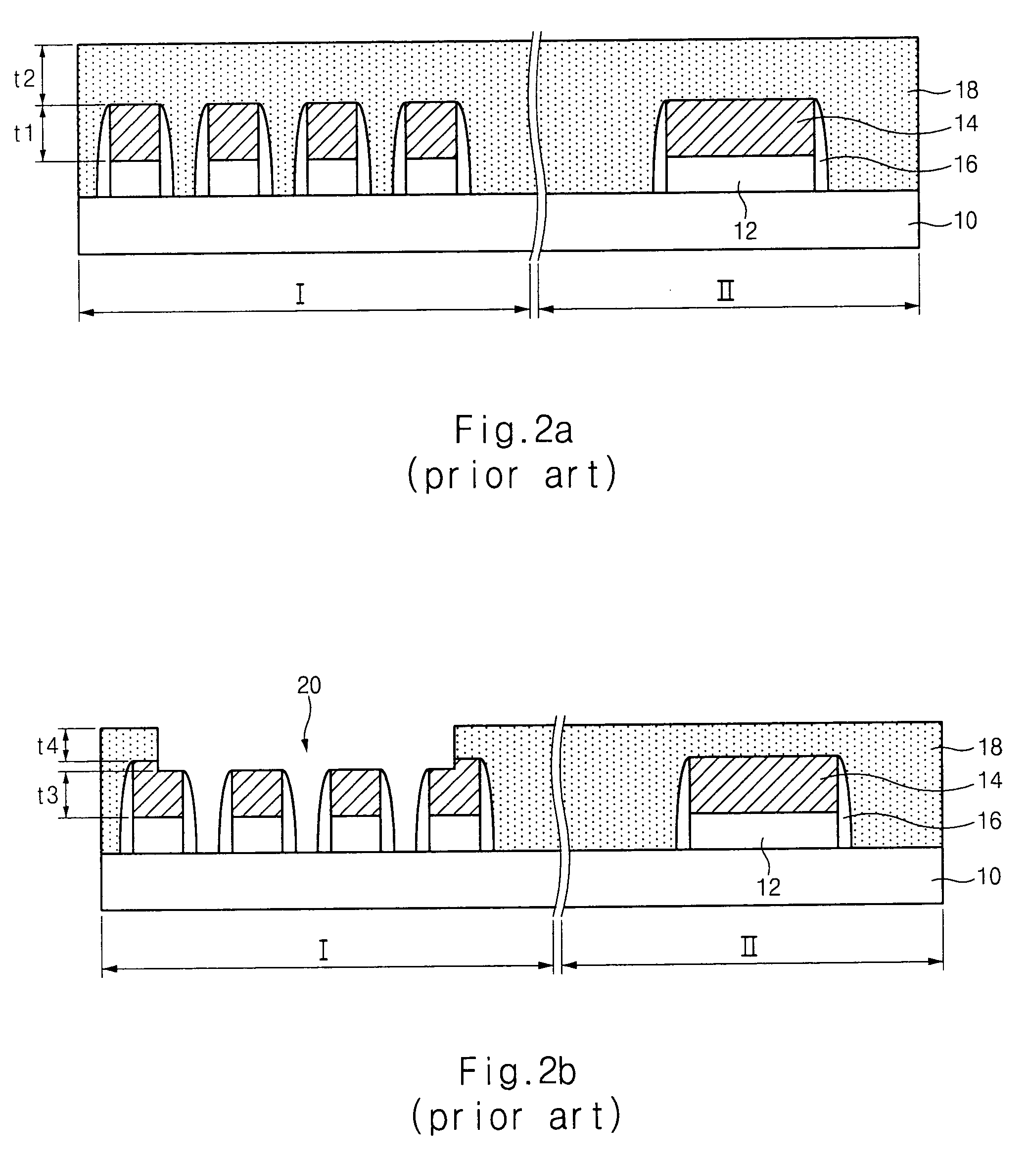
As described above, when the word line is exposed, misalignment is generated in a subsequent process, and a bridge is formed between a word line wire and a storage node contact or leakage current increases, which result in failure of the device.
However, as semiconductor devices are required to have higher densities, reduction of the size of devices and insulation between devices became more difficult when the LOCOS process is used.
However, a lot of scratches 21 are formed in the polished region because the particles of CeO2 are large and rough.
Such scratches cause failure of the device, and thus reduce a yield of the device.

Method used


Image

  • CMP slurry for semiconductor device, and method for manufacturing semiconductor device using the same
  • CMP slurry for semiconductor device, and method for manufacturing semiconductor device using the same
  • CMP slurry for semiconductor device, and method for manufacturing semiconductor device using the same

Examples


example 1

[0113] To 40 wt % of slurry for an oxide film (Cabot, SS-25) including fumed SiO2 having a size of 20 to 300 nm were added 55 wt % of deionized water and 5 wt % of sodium stearate with stirring. And the resulting mixture was further stirred for about 30 minutes to be completely mixed and stabilized, to prepare a slurry of pH 6. Here, the content of the fumed SiO2 was 10 wt % based on the total weight of the prepared slurry.

example 2

[0114] To 60 wt % of slurry for an oxide film (Bayer, LEVASIL 50CK / 30% V1) including colloidal SiO2 having a size of 20 to 300 nm were added 1 wt % of sodium lauric sulfate with stirring and 39 wt % of deionized water. And the resulting mixture was further stirred for about 30 minutes to be completely mixed and stabilized, to prepare a slurry of pH 3. Here, the content of the colloidal SiO2 was 18 wt % based on the total weight of the prepared slurry.

example 3

[0115] To 80 wt % of slurry for an oxide film including Al2O3 having a size of 20 to 300 nm were added 10 wt % of dodecyl benzene sulfonate with stirring and 10 wt % of deionized water. And the resulting mixture was further stirred for about 30 minutes to be completely mixed and stabilized, to prepare a slurry of pH 5. Here, the content of the Al2O3 was 10 wt % based on the total weight of the prepared slurry.


PUM

PropertyMeasurementUnit
sizeaaaaaaaaaa
pressureaaaaaaaaaa
thicknessaaaaaaaaaa

Abstract

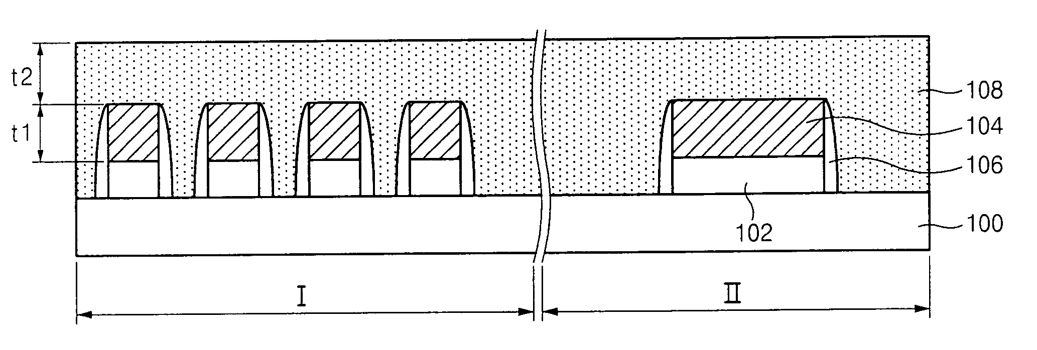
A CMP slurry for a semiconductor device and a method for manufacturing the semiconductor device using the same, more specifically, a slurry including an additive having high affinity to a nitride film, and a method for polishing a complex film consisting of a polysilicon film and an oxide film or an oxide film using the same are described herein. When the complex film consisting of the polysilicon film and the oxide film removed by using the CMP slurry, a hard mask film which is the nitride film is not removed. Therefore, a polysilicon plug of the semiconductor device can be formed without exposing a word line electrode. In addition, when the oxide film is removed by using the CMP slurry, the slurry includes Al or SiO2 having spherical shaped particles as an abrasive, to form an STI type device isolation film which does not have scratches.

Description

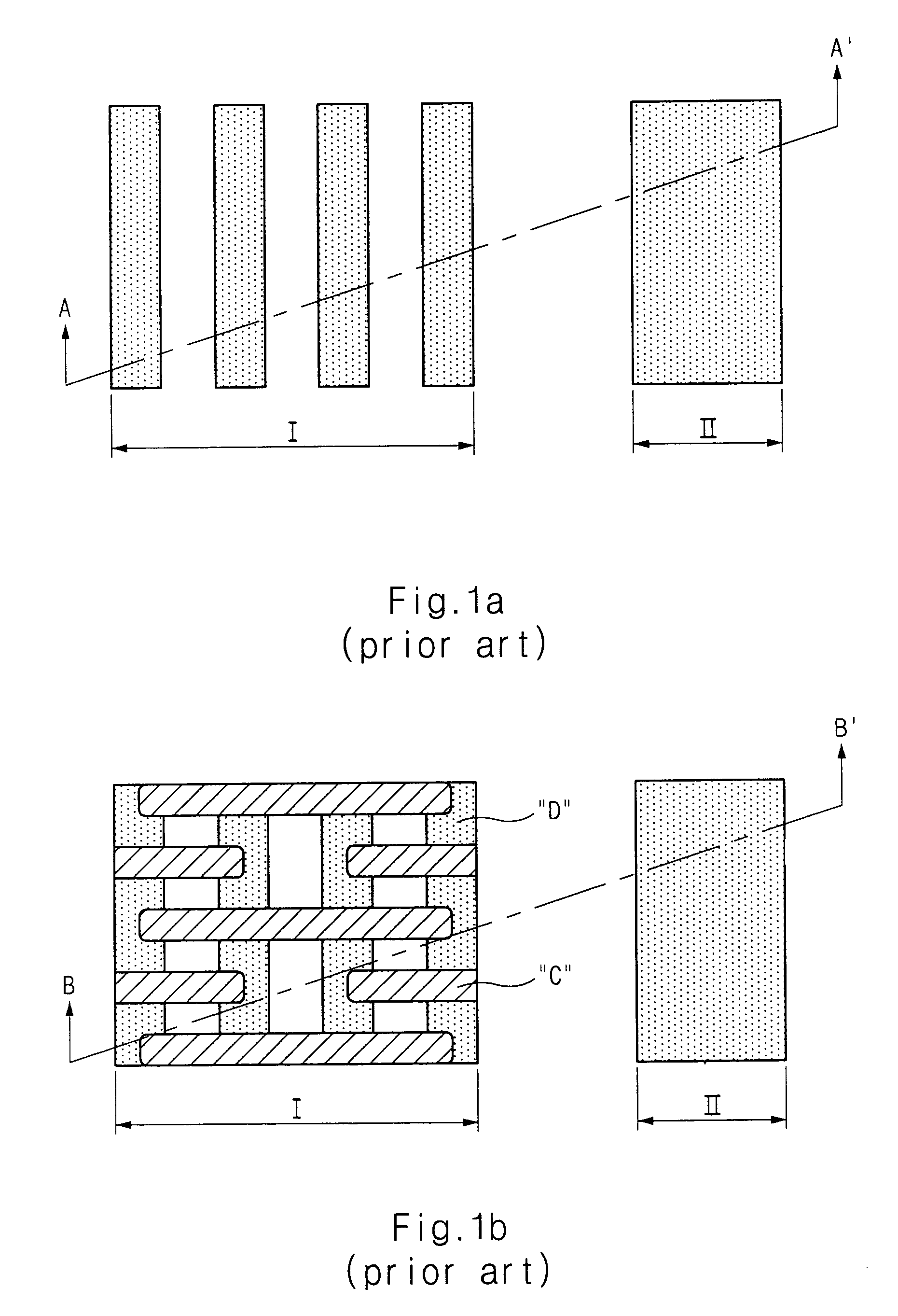
TECHNICAL FIELD[0001] The present disclosure relates to a chemical mechanical polishing (CMP) slurry for a semiconductor device and a method for manufacturing the semiconductor device using the same, and more particularly to a method for forming a polysilicon plug by removing a complex film consisting of a polysilicon film and an oxide film, or forming an STI type device isolation film by removing an oxide film via a CMP process using a slurry including an additive having high affinity to a nitride film.[0002] In general, a polysilicon plug has been used as a contact plug for manufacturing a high integration semiconductor device. The polysilicon plug is formed by depositing a polysilicon film on the whole surface of a semiconductor substrate on which a contact hole has been formed, and performing a CMP process on the polysilicon film.[0003] FIG. 1a is a top plan view after formation of a word line, FIG. 1b is a top plan view after formation of a polysilicon plug contact, and FIGS. 2...

Claims


Application Information

Patent Timeline
Patent Type & Authority Applications(United States)
IPC IPC(8): C09C1/68C09G1/02C09K3/14H01L21/3105H01L21/318H01L21/321H01L21/60H01L21/762H01L21/768
CPCC09G1/02C09K3/1463H01L21/31053H01L21/3185H01L21/76897H01L21/76229H01L21/76232H01L21/76819H01L21/7684H01L21/3212H01L21/0217
Inventor JUNG, JONG GOOPARK, HYUNG SOON
Owner SK HYNIX INC
Why Eureka
Try Eureka