Low latency fifo circuit for mixed clock systems

Inactive Publication Date: 2004-07-01
THE TRUSTEES OF COLUMBIA UNIV IN THE CITY OF NEW YORK
View PDF9 Cites 28 Cited by
  • Summary
  • Abstract
  • Description
  • Claims
  • Application Information

AI Technical Summary

Problems solved by technology

A challenging problem is to robustly interface these domains.
There have been few adequate solutions, especially ones providing reliable low-latency communication.
Some designs are limited to handling single-clock systems.
However, the latency of his design is proportional with the number of FIFO stages, whose implementation includes expensive synchronizers.
However, these designs temporarily modify the receiver's clock.
This approach changes the local systems' clocks, and may introduce latency penalties in restarting them.
If it is deasserted, the put interface is stalled.
In practice, however, the two interfaces will often not be cooperative and the FIFO may become empty or full.
This situation potentially creates synchronization problems.
A problem is for the sender to see a "clean" full signal, i.e., synchronized to its own clock, and not the actual value of that signal.
However, this synchronization in turn introduces additional latencies that may result in data inconsistencies (overflow and underflow

Method used


Image

  • Low latency fifo circuit for mixed clock systems
  • Low latency fifo circuit for mixed clock systems
  • Low latency fifo circuit for mixed clock systems

Examples


Embodiment Construction

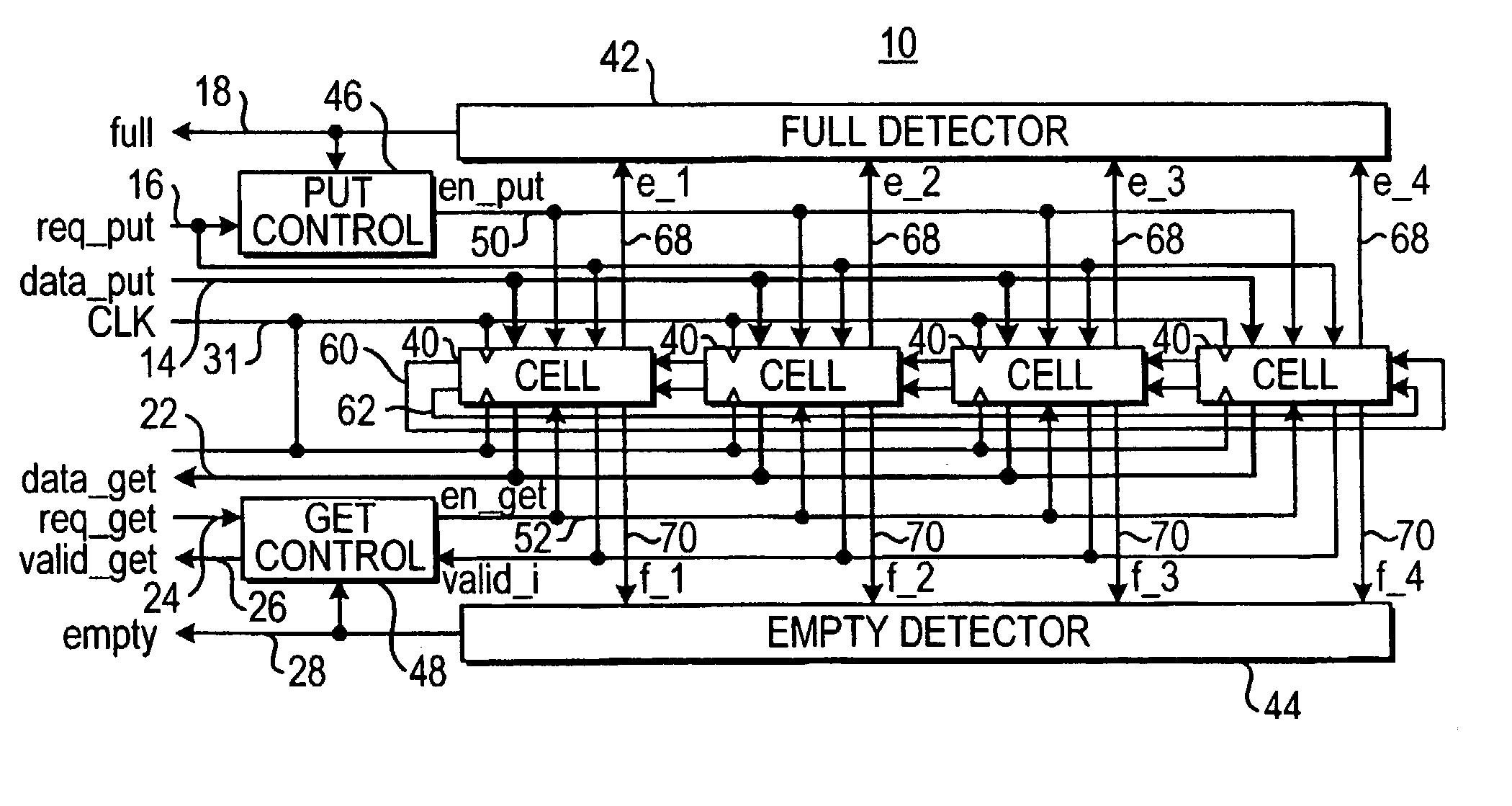
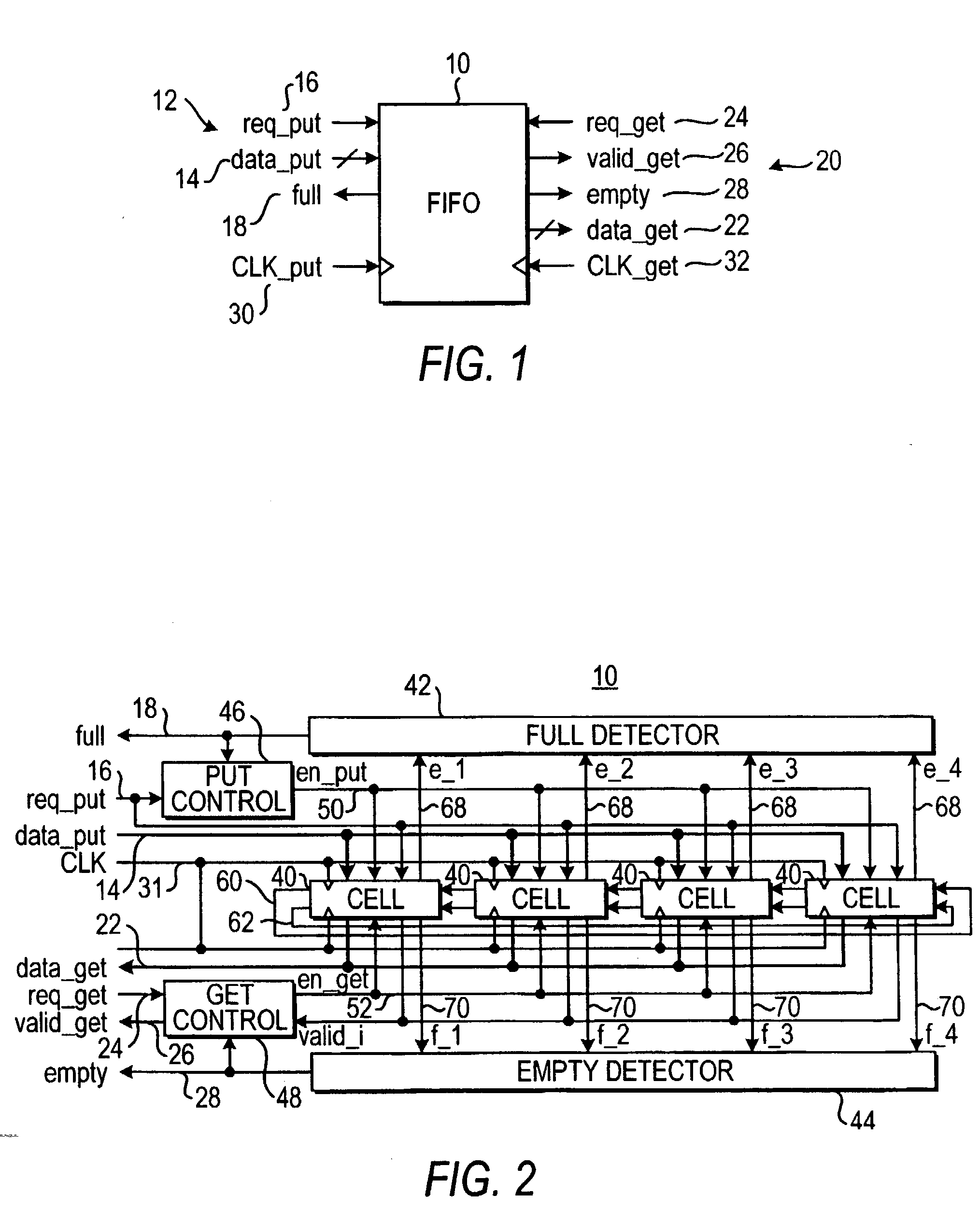
[0083] In order to evaluate the performance of the various FIFO designs presented in this paper, the circuits were simulated using HSpice (.COPYRGT. Avant! Corporation), assuming implementation in 0.6 .mu.m HP CMOS technology at 3.3V at and 300K.

[0084] The behavior of a FIFO of capacity 8, with a data item of width 8 was simulated. For en.sub.put, req.sub.put, en.sub.get and data.sub.put, buffering was used to drive the capacitance of all cells. For valid.sub.i and data.sub.put, in addition to the load provided by the appropriate latching / result logic, a load contributed by long wires was modeled. The wire load was estimated to be equivalent to two inverters per cell.

[0085] The results for the maximum clock frequencies at which each circuit can be clocked are presented in Table 1.

1TABLE 1 Maximum clocking frequencies Version CLK.sub.in CLK.sub.out Single Clock 10 584 MHz Mixed Clocks 100 523 MHz 554 MHz Relay Station 300 562 MHz 552 MHz

[0086] All of the designs were clocked to over ...


PUM


Abstract

A FIFO design interfaces a sender subsystem and a receiver subsystem operating on different time domains. The sender subsystem and the receiver subsystem may be synchronous or asynchronous. The FIFO circuit includes a put interface configured to operate in accordance with the sender time domain and get interface configured to operate in accordance with the receiver time domain. The FIFO circuit includes an array of cells having a register and state controller indicative of the state of the cell. Each cell also has a put component part configured to operate according to the sender time domain including a put token passing circuit and put controller circuit. Each cell has get component part configured to operate according to the receiver time domain including a get token passing circuit and a get controller circuit. A mixed-clock relay station design interfaces a sender subsystem and a receiver subsystem working at different time domains, and where the latency between sender and receiver is large.

Description

[0001] This application claims priority to U.S. Provisional Patent Application entitled "A Low-Latency FIFO For Mixed-Clock Systems," Serial No. 60 / 199,851, which was filed on Apr. 26, 2000, which is incorporated by reference in its entirety herein.[0002] 1. Field of the Invention[0003] This invention relates to FIFO circuits, and more particularly to low latency FIFO designs that interface subsystems working at different speeds or between subsystems with very long interconnection delays.[0004] 2. Background of Related Art[0005] A trend in VLSI is increasingly towards a "system-on-a-chip" involving many clock domains. A challenging problem is to robustly interface these domains. There have been few adequate solutions, especially ones providing reliable low-latency communication.[0006] A number of FIFO designs and components have been developed to handle timing discrepancies between subsystems. Some designs are limited to handling single-clock systems. These approaches have been prop...

Claims


Application Information

Patent Timeline
IPC IPC(8): G06F5/10G06F5/12G06F13/40G11C29/00
CPCG06F5/12G06F13/4036G06F2213/0038G06F2205/126G06F13/4059
Inventor CHELCEA, TIBERIUNOWICK, STEVEN M.
Owner THE TRUSTEES OF COLUMBIA UNIV IN THE CITY OF NEW YORK
Why Eureka
Try Eureka