Method for forming conductive wires of semiconductor device

a technology of conductive wires and semiconductor devices, which is applied in the direction of semiconductor devices, basic electric elements, electrical equipment, etc., can solve the problems of lithography overlay, difficult etching of copper wires using conventional etching materials, and known methods having problems with lithography overlay,

Inactive Publication Date: 2004-08-19
KEY FOUNDRY CO LTD
View PDF1 Cites 153 Cited by
  • Summary
  • Abstract
  • Description
  • Claims
  • Application Information

AI Technical Summary

Problems solved by technology

However, copper wires are difficult to etch using conventional etching materials.
Unfortunately, known methods have problems with lithography overlays, especially in semiconductor devices utilizing a design rule 0.13 .mu.m.
Using a design rule of 0.13 .mu.m or below often results in misalignment of via / contact holes of up to 0.01 .mu.m.
It is difficult to control misalignment under 0.03 .mu.m, especially using a stepper.
Thus, conventional damascene processes must be performed with many restrictions.
In addition, the stepper itself has limits on overlays, since misalignment of the hole and the trench often occurs.
As explained above, traditional methods for forming conductive wires in semiconductor devices often cause misalignments during formation of the trench and the via / contact hole, and exhibits the problems shown in FIGS. 2a through 2c, i.e., poisoning, facet, and attachment of etching byproducts, which cause lower process yields and may lower reliability of the semiconductor device.

Method used


Image

  • Method for forming conductive wires of semiconductor device
  • Method for forming conductive wires of semiconductor device
  • Method for forming conductive wires of semiconductor device

Examples


Embodiment Construction

[0026] Reference will now be made in detail to exemplary embodiments of the invention, examples of which are illustrated in the accompanying drawings. Wherever possible, the same reference numbers will be used throughout the drawings to refer to the same or like parts.

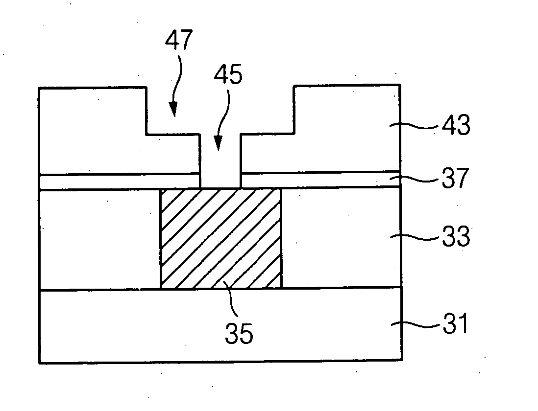
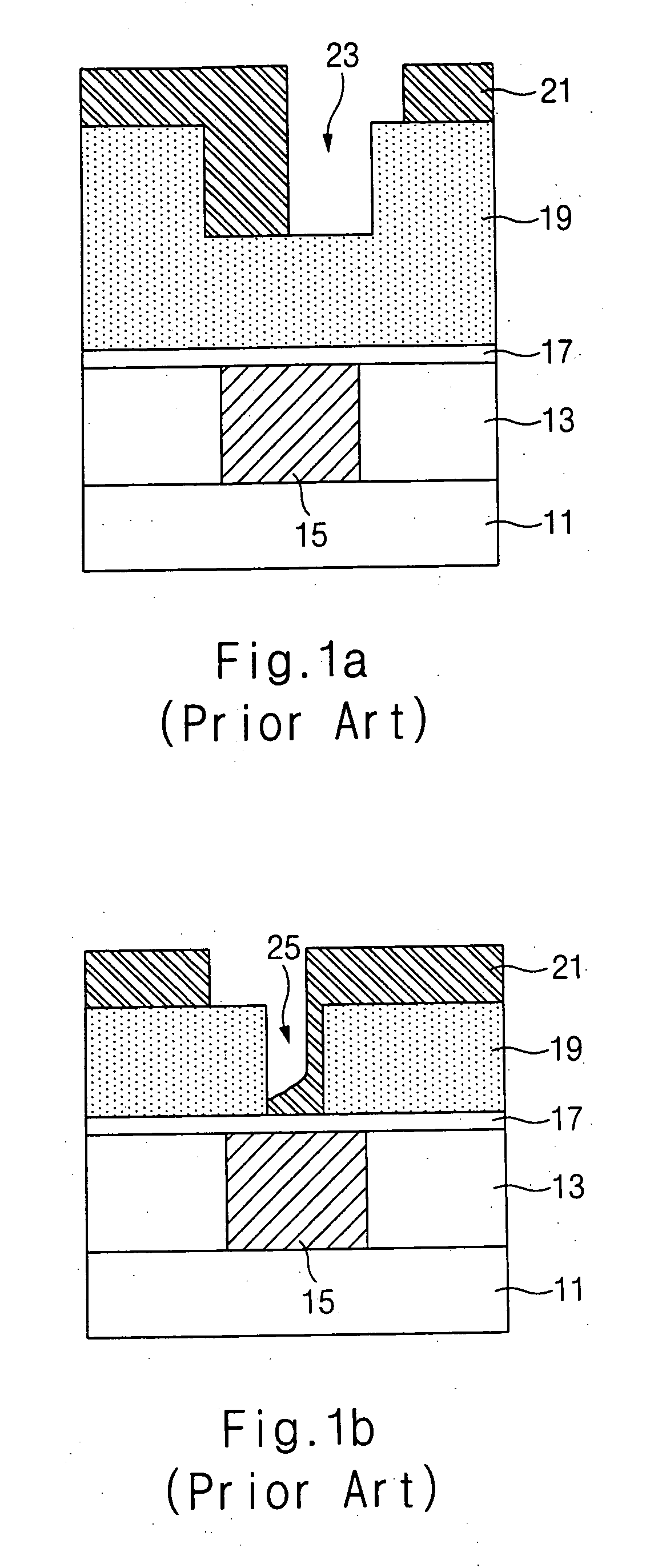
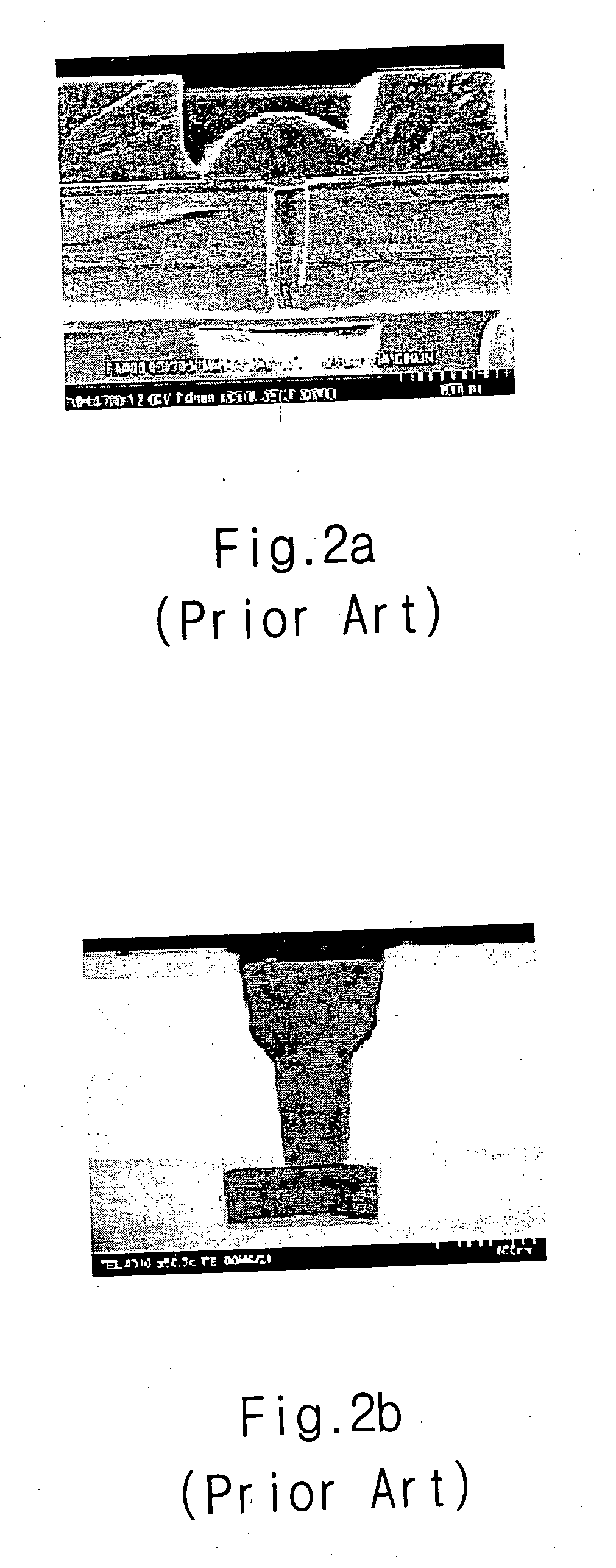
[0027] Conductive wires of a semiconductor device may be formed, for example, to prevent misalignment and improve the device's electric characteristics. Engraved polycrystalline silicon patterns are formed where a via / contact plug and an upper metal wire are located based on a notching phenomenon. The notching phenomenon uses the different etching selectivity between the polycrystalline silicon layer and lower film.

[0028] When the etching selectivity ratio between a polycrystalline silicon layer and a lower film is 5:1 to 500:1, a notching phenomenon may occur during the etching process of the polycrystalline silicon layer. The notching phenomenon allows an engraved polycrystalline silicon layer pattern to form on the ...


PUM

PropertyMeasurementUnit
temperatureaaaaaaaaaa
thicknessaaaaaaaaaa
temperatureaaaaaaaaaa

Abstract

A method is provided for forming a conductive wire of a semiconductor device using, for example, a damascene process. A conductive wire, such as a metal wire, is formed, based on a notching phenomenon which occurs when the etching selectivity between a polycrystalline silicon layer and a lower film is approximately 5 to 500:1.

Description

[0001] 1. Field of the Invention[0002] The present invention relates to a method for forming conductive wires of a semiconductor device, more particularly, to a method for forming conductive wires of a semiconductor device by utilizing a notching phenomenon of polycrystalline silicon.[0003] 2. Description of the Related Art[0004] Semiconductor fabrication techniques attempt to attain high integration and high performance. Copper wiring is commonly used in the fabrication of semiconductor devices.[0005] However, copper wires are difficult to etch using conventional etching materials. Due to this characteristic of copper wires, a damascene process is typically used in which an interlayer dielectric film is etched to form a trench, a copper layer is deposited to fill the trench, and the copper layer is then planarized.[0006] There are various known methods for forming copper wires using the damascene process. For example, in one known process a trench is formed for the copper wire, and...

Claims


Application Information

Patent Timeline
Patent Type & Authority Applications(United States)
IPC IPC(8): H01L21/3065H01L21/768H01L21/28
CPCH01L2221/1026H01L21/76807H01L21/28
Inventor RYU, SANG WOOK
Owner KEY FOUNDRY CO LTD
Why Eureka
Try Eureka