Light guide for image sensor

Active Publication Date: 2004-09-16
TAIWAN SEMICON MFG CO LTD
View PDF8 Cites 81 Cited by
  • Summary
  • Abstract
  • Description
  • Claims
  • Application Information

AI Technical Summary

Problems solved by technology

The light scattering problem causes degraded image resolution for black and white sensors or complicated color correction for color sensors.
However

Method used


Image

  • Light guide for image sensor
  • Light guide for image sensor
  • Light guide for image sensor

Examples


Embodiment Construction

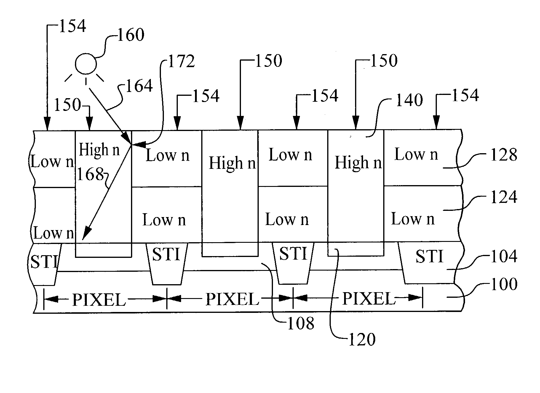
[0021] The preferred embodiments of the present invention disclose a method to form an image sensor array device. The device uses dielectric layers having differing indexes of refraction to create light guides and light shields for each pixel in the array. This method prevents light cross talk. It should be clear to those experienced in the art that the present invention can be applied and extended without deviating from the scope of the present invention.

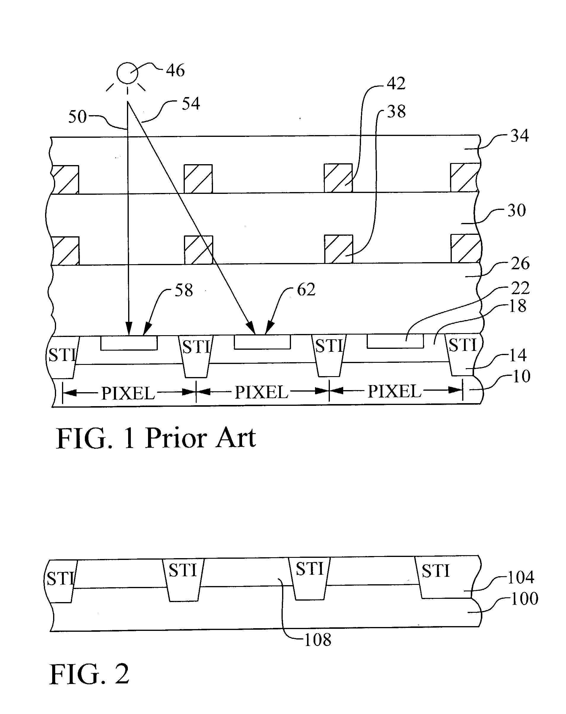
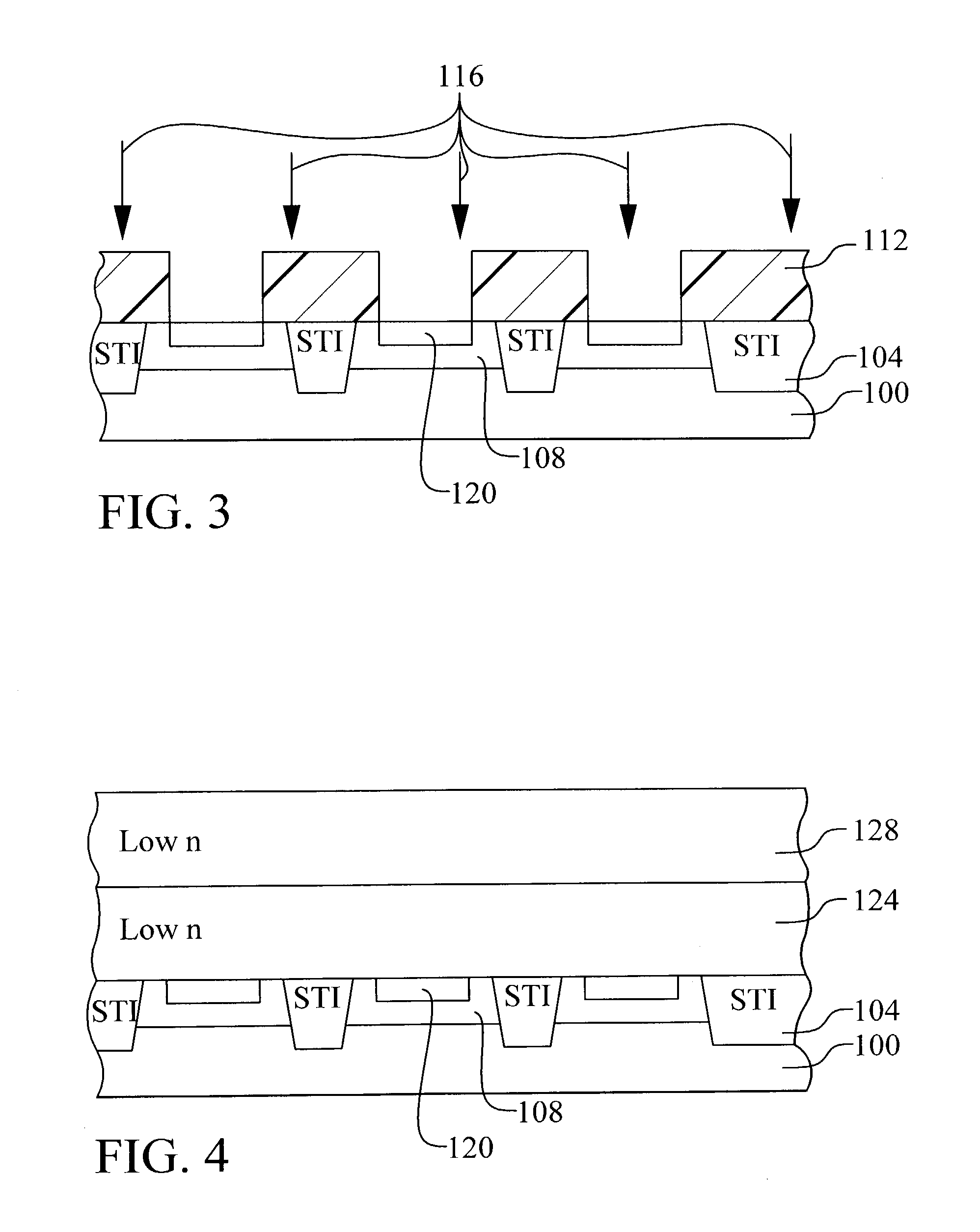
[0022] Referring now to FIG. 2, the preferred embodiment of the present invention is illustrated. Several important features of the present invention are shown therein and discussed below. The embodiments of the present invention are applied to the formation of a unique, image sensor array comprising a plurality of diodes formed in a semiconductor substrate. The teachings may be further applied to any form of image sensing array.

[0023] In particular, a substrate 100 is provided. The substrate 100 preferably comprises a semiconducto...


PUM


Abstract

A new method to form an image sensor device is achieved. The method comprises forming an image sensing array in a substrate comprising a plurality of light detecting diodes with spaces between the diodes. A first dielectric layer is formed overlying the diodes but not the spaces. The first dielectric layer has a first refractive index. A second dielectric layer is formed overlying the spaces but not the diodes. The second dielectric layer has a second refractive index that is larger than the first refractive index. A new image sensor device is disclosed.

Description

[0001] (1) Field of the Invention[0002] The invention relates to solid state image sensors, and, more particularly, to a method to form light guides for an image sensor to eliminate cross talk between pixels.[0003] (2) Description of the Prior Art[0004] Light imaging array devices are used in a wide variety of applications. These devices utilize an array of active, semiconductor devices, such as diodes, to convert images into streams of digital data.[0005] Referring now to FIG. 1, a prior art image sensor device is illustrated in cross section. This device comprises a semiconductor substrate 10 onto which an array of diodes is formed. Each diode comprises, for example, an n-type region 22 in a p-type region 18. Each diode is separated from other diodes in the array by isolation regions 14 to thereby form an array of pixels. The pixels are used to convert incoming light 50 and 54 from a light / image source 46 into electrical signals via the photo-diodes.[0006] Typically, the substrate...

Claims


Application Information

Patent Timeline
IPC IPC(8): H01L21/00H01L27/146
CPCH01L27/14685H01L27/14625
Inventor YAUNG, DUN-NIANWUU, SHOU-GWOCHIEN, HO-CHINGTSENG, CHIEN-HSIEN
Owner TAIWAN SEMICON MFG CO LTD
Why Eureka
Try Eureka