AC/DC flyback converter

a converter and input current technology, applied in the field of improved single-stage inputcurrent shaping flyback converters, can solve the problems of increasing line current harmonics, reducing input power factor and reducing total harmonic distortion (thd), and not improving power factor (pf) and reducing thd as much as their two-stage counterparts,

Active Publication Date: 2004-12-16
DELTA ELECTRONICS INC
View PDF8 Cites 111 Cited by
  • Summary
  • Abstract
  • Description
  • Claims
  • Application Information

AI Technical Summary

Problems solved by technology

Generally, S.sup.2ICS converters meet European and / or Japanese regulatory requirements regarding the line-current harmonic limits, but they do not improve the power factor (PF) and reduce the total harmonic distortion (THD) as much as their two-stage counterparts.
However, a larger inductance of inductor 101 also decreases input power factor and increases line current harmonics.
However, the DCM operation of the ICS inductor results in a larger current stress on switch 108 and larger input-current ripple.
However, interleaving of two converters significantly increases the number of components.
Furthermore, if the flyback transformer operates at the DCM / CCM boundary, interleaving of variable-frequency converters requires a relatively complex control circuit.

Method used


Image

  • AC/DC flyback converter
  • AC/DC flyback converter
  • AC/DC flyback converter

Examples


Embodiment Construction

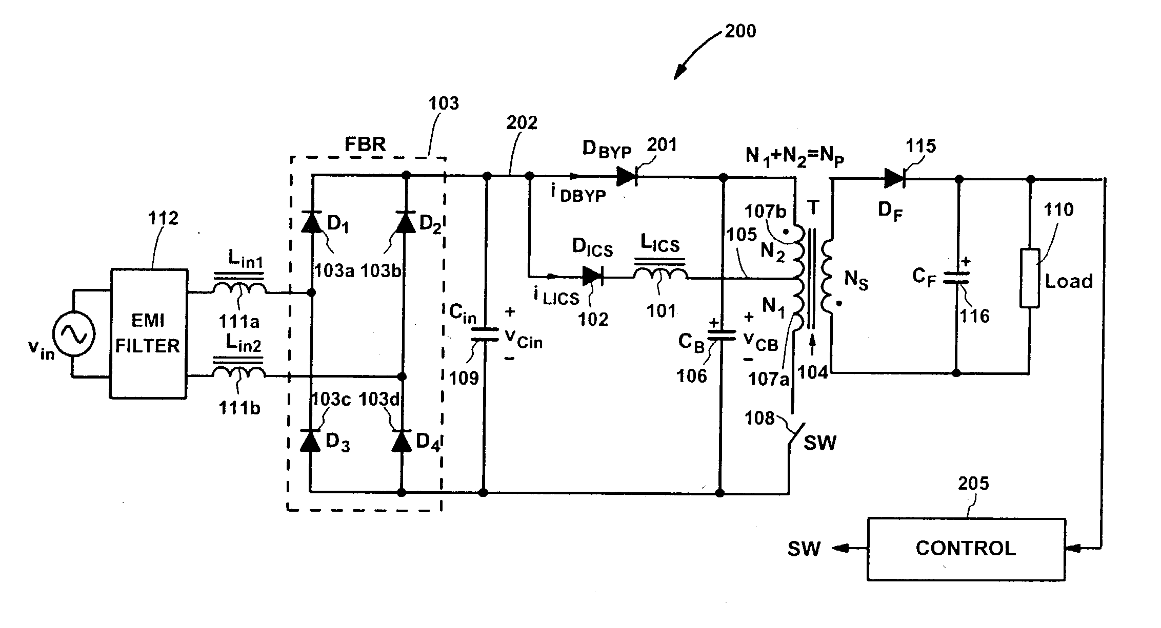
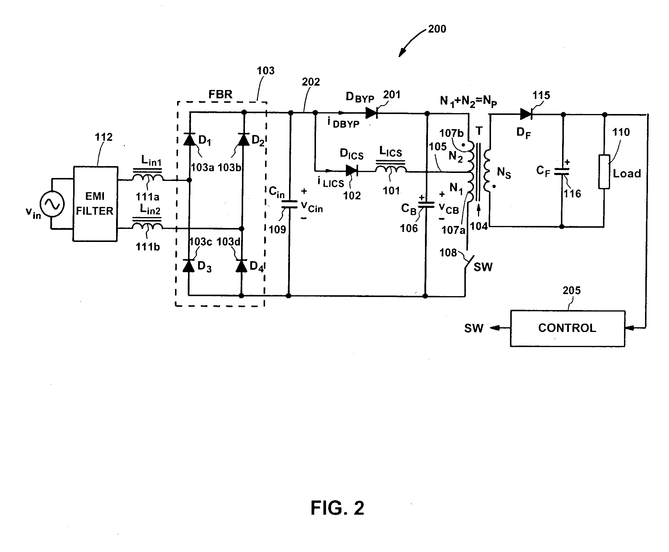
[0038] FIG. 2 is a circuit diagram of S.sup.2ICS flyback converter 200, according to one embodiment of the present invention. As shown in FIG. 2, S.sup.2ICS flyback converter 200 is substantially the same as S.sup.2ICS flyback converter 100 of FIG. 1, except that bypass diode 201 (D.sub.BYP) is connected between the positive terminal of full-bridge rectifier (FBR) 103 and the positive terminal of energy-storage (bulk) capacitor 106 (C.sub.B). A control circuit 205 provides a control signal SW for periodically opening and closing switch 108, according to a switching control scheme. One such scheme, for example, opens and closes switch 108 at a variable frequency such that transformer 104 operates at the boundary between discontinuous and continuous conduction modes. Secondary-side rectifier 115 can be implemented either with a Schottky rectifier or with a synchronous rectifier.

[0039] FIGS. 3(a), 3(b) and 3(c) illustrate the basic operation of bypass diode 201 and the effects of diode...


PUM


Abstract

A single-stage input-current-shaping (S<2>ICS) flyback converter achieves substantially reduced conduction losses in the primary side of the S<2>ICS flyback converter by connecting a bypass diode between the positive terminal of a full-bridge rectifier and the positive terminal of an energy-storage capacitor. An effective current interleaving between an energy-storage inductor and the bypass diode is thus obtained in the S<2>ICS flyback converter around the peak of the rectified line voltage, resulting in a significantly reduced input-current ripple and reduced current stress on the switch. Further, by rearranging the rectifiers in the ICS part of the S<2>ICS flyback converter in such a way that the energy-storage capacitor and the ICS inductor are connected to the ac line voltage through only two rectifiers, one diode forward-voltage drop is eliminated, which results in a substantially reduced conduction loss in the primary-side rectifiers.

Description

BACKGOUND OF THE INVENTION[0001] 1. Field of the Invention[0002] This invention relates to an improved single-stage input-current-shaping flyback converter with fast output-voltage regulation, and, more particularly, to a single-stage, single-switch input-current-shaping flyback converter with reduced conduction losses in the primary side of the converter.[0003] 2. Discussion of the Related Art[0004] In single-stage input-current-shaping (S.sup.21CS) converters, input-current shaping (ICS), isolation, and high-bandwidth output-voltage control are performed in a single conversion step (i.e., without creating a regulated DC bus, as is commonly found in two-stage ICS converters). Most of the S.sup.2ICS circuits integrate a boost ICS stage with a forward or flyback DC / DC-converter stage. Generally, S.sup.2ICS converters meet European and / or Japanese regulatory requirements regarding the line-current harmonic limits, but they do not improve the power factor (PF) and reduce the total harm...

Claims


Application Information

Patent Timeline
Patent Type & Authority Applications(United States)
IPC IPC(8): H02M1/00H02M3/28H02M1/42
CPCY02B70/126H02M1/4258Y02B70/10
Inventor HUBER, LASZLOJOVANOVIC, MILAN M.CHANG, CHIEN-CHUNG
Owner DELTA ELECTRONICS INC
Why Eureka
Try Eureka