Matching device and plasma processing apparatus

a matching device and plasma technology, applied in the direction of waveguide type devices, plasma techniques, coatings, etc., can solve the problem of increasing the axial ratio of the circularly polarized wave, and achieve the effect of convenient accurate control

Inactive Publication Date: 2004-12-30
TOKYO ELECTRON LTD +1
View PDF5 Cites 27 Cited by
  • Summary
  • Abstract
  • Description
  • Claims
  • Application Information

AI Technical Summary

Benefits of technology

0013] The present invention has been made to solve the above problems, and has as its object to provide a matching device capable of easily performing accurate control.

Problems solved by technology

Unfortunately, if the microwave is reflected in the processing vessel or RLSA, enters the cylindrical waveguide form the RLSA, and is reflected again, the axial ratio of the circularly polarized wave increases by the influence of this reflection.

Method used


Image

  • Matching device and plasma processing apparatus
  • Matching device and plasma processing apparatus
  • Matching device and plasma processing apparatus

Examples


first embodiment

[0061] First Embodiment

[0062] A plasma processing apparatus using a matching device of the present invention has a processing vessel which accommodates an object to be processed and performs plasma processing for this object, and an electromagnetic field supply apparatus which supplies a microwave into this processing vessel and generates a plasma in the processing vessel by the action of the electromagnetic field of the microwave. The arrangements of the processing vessel and electromagnetic field supply apparatus of the plasma processing apparatus of the first embodiment of the present invention will be separately described below.

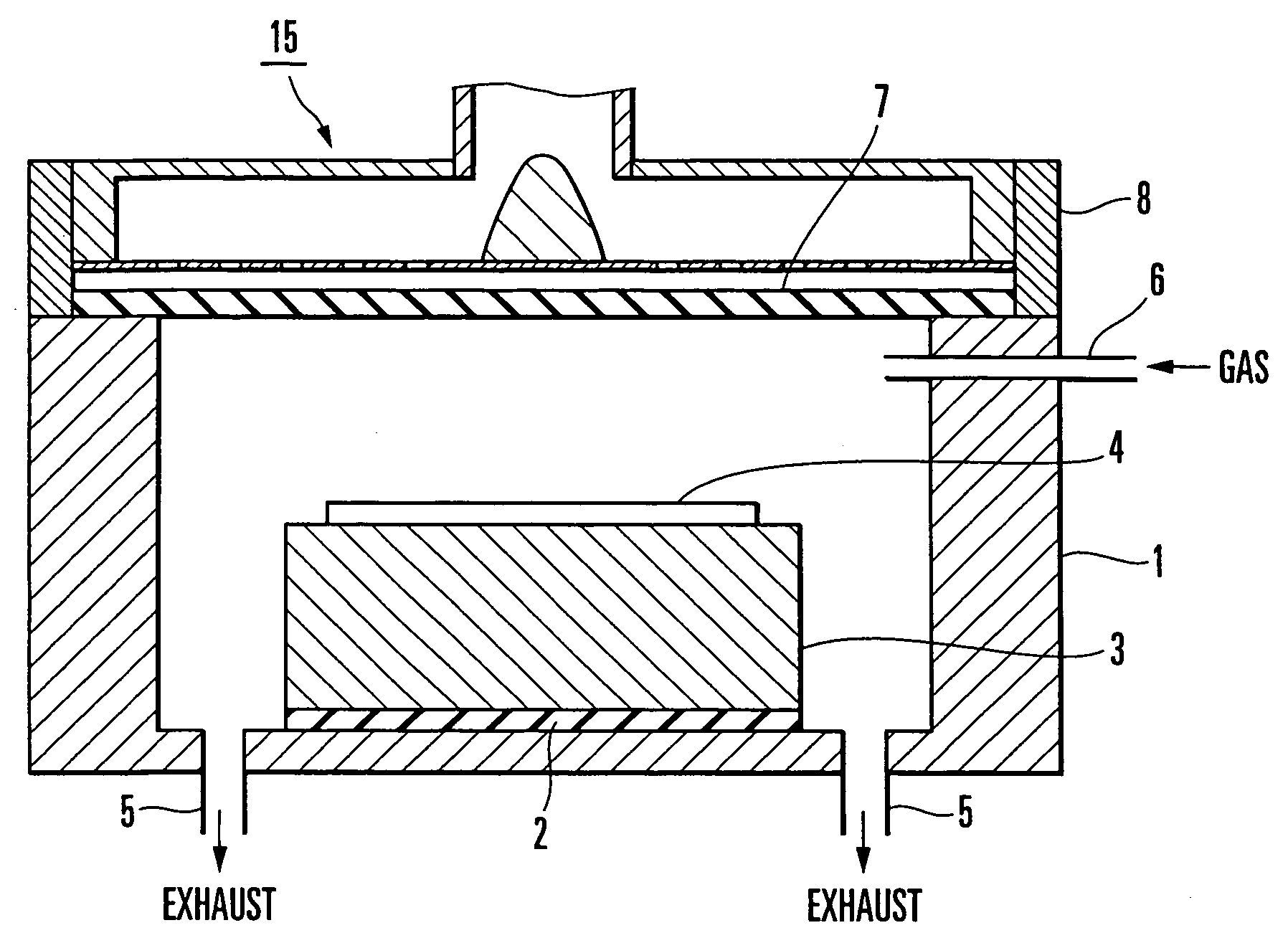
[0063] FIG. 1 is a sectional view showing the arrangement of the processing vessel.

[0064] A processing vessel 1 has a closed-end cylindrical shape having an open upper portion. A substrate table 3 is fixed via an insulating plate 2 to a central portion of the bottom surface of the processing vessel 1. On the upper surface of the substrate table 3, a subst...

second embodiment

[0098] Second Embodiment

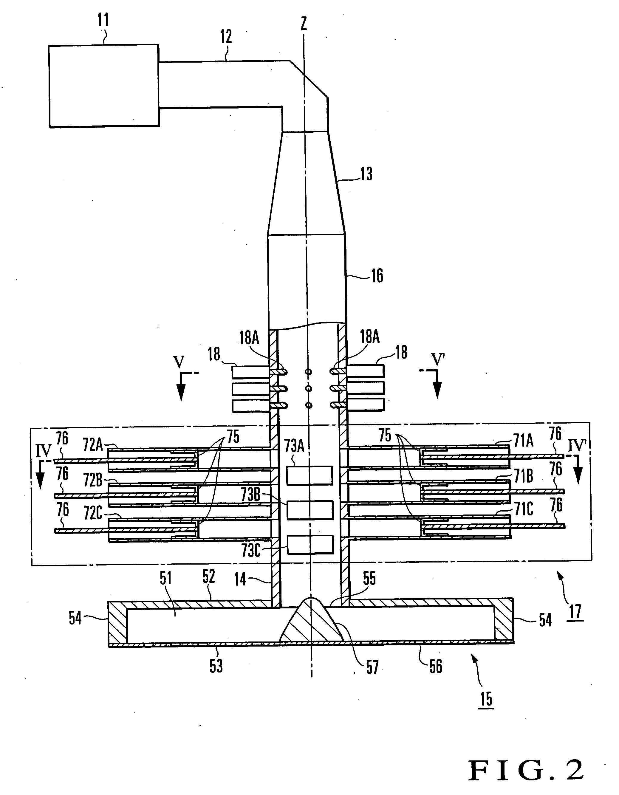
[0099] FIG. 10A is a sectional view showing the arrangement of a matching device of the second embodiment of the present invention, and shows a sectional arrangement including the axis (Z) of a cylindrical waveguide having this matching device. FIG. 10B is a sectional view, taken along a line Xb-Xb' in FIG. 10A, showing a sectional arrangement in a plane (X-Y plane) perpendicular to the axis (Z) of the cylindrical waveguide. The same reference numerals as in FIGS. 2 and 4 denote the same parts in FIGS. 10A and 10B, and an explanation thereof will be suitably omitted.

[0100] A matching device 117 shown in FIGS. 10A and 10B match the impedances of the supply side and load side of a cylindrical waveguide 14, and uses a plurality of stabs 171A to 171C, 172A to 172C, 173A to 173C, and 174A to 174C (the stabs 174B and 174C are not shown) as reactance elements. Each of the stabs 171A to 174C is a rod having a circular section and a tip rounded into a substantially sp...

third embodiment

[0112] Third Embodiment

[0113] FIG. 11 is a sectional view showing the arrangement of a matching device of the third embodiment of the present invention, and shows a sectional arrangement including the axis (Z) of a cylindrical waveguide having this matching device. FIG. 12 is a sectional view, taken along a line XII-XII' in FIG. 11, showing a sectional arrangement in a plane (X-Y plane) perpendicular to the axis (Z) of the cylindrical waveguide. The same reference numerals as in FIGS. 2 and 4 denote the same parts in FIGS. 11 and 12, and an explanation thereof will be suitably omitted.

[0114] Similar to the matching device 117 shown in FIGS. 10A and 10B, a matching device 217 shown in FIGS. 11 and 12 is made up of stabs (first stabs) 271A to 271C, stabs (third stabs) 272A to 272C, stabs (second stabs) 273A to 273C, and stabs (fourth stabs) 274A to 274C (the stabs 274B and 274C are not shown).

[0115] The matching device 217, however, differs from the matching device 117 shown in FIGS. ...


PUM

PropertyMeasurementUnit
angleaaaaaaaaaa
relative dielectric constantaaaaaaaaaa
dielectric constantaaaaaaaaaa

Abstract

A machining device includes first branched waveguides (71A-71C) and second branched waveguides (73A-73C) connected perpendicularly to an axial (Z) direction of a cylindrical waveguide (14) and having one end which opens in the cylindrical waveguide (14) and the other end which is electrically short-circuited. The first branched waveguides (71A-71C) are arranged at a predetermined interval in an axial (z) direction of the cylindrical waveguide (14). The second branched waveguides (73A-73C) are arranged in positions which make an angle of 90° with positions of the first branched waveguides (71A-71C) when viewed from the axis (Z) of the cylindrical waveguide (14), and arranged at a predetermined interval in the axial (Z) direction of the cylindrical waveguide (14). With this arrangement, it is possible to accurately and easily control the impedance matching between the supply side and load side of the cylindrical waveguide (14).

Description

[0001] The present invention relates to a matching device and, more particularly, to a matching device for matching the impedances of the supply side and load side of a cylindrical waveguide.[0002] The present invention also relates to a plasma processing apparatus and, more particularly, to a plasma processing apparatus for generating a plasma by using a high-frequency electromagnetic field, and processing an object to be processed such as a semiconductor or LCD (Liquid Crystal Display).[0003] In the fabrication of semiconductor devices and flat panel displays, plasma processing apparatuses are often used to form oxide films and perform crystal growth, etching, and ashing of semiconductor layers. One of these plasma processing apparatuses is a microwave plasma processing apparatus which generates a plasma by supplying a microwave from a radial line slot antenna (to be abbreviated as an RLSA hereinafter) into a processing vessel, and ionizing and dissociating a gas in the processing...

Claims


Application Information

Patent Timeline
Patent Type & Authority Applications(United States)
IPC IPC(8): H05H1/46H01J37/32H01L21/205H01L21/302H01L21/3065H01L21/31H01P5/04
CPCH01J37/32192H01J37/32256H01P5/04
Inventor ISHII, NOBUOSHINOHARA, KIBATSU
Owner TOKYO ELECTRON LTD
Why Eureka
Try Eureka