

Two-port isolator and communication device
a technology of isolators and communication devices, applied in waveguide devices, basic electric elements, electrical apparatus, etc., can solve the problems of high insertion loss, high power loss, and increase the production cost of isolators of high-q dielectric materials
Active Publication Date: 2004-12-30
MURATA MFG CO LTD
View PDF0 Cites 22 Cited by
- Summary
- Abstract
- Description
- Claims
- Application Information
AI Technical Summary
Benefits of technology
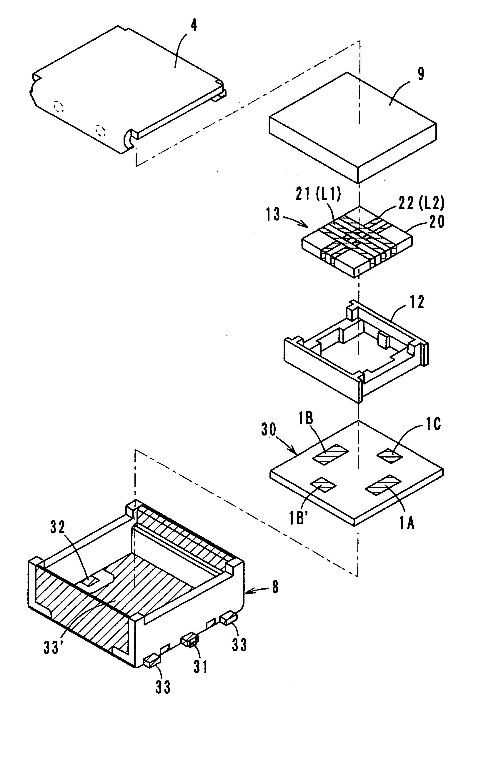
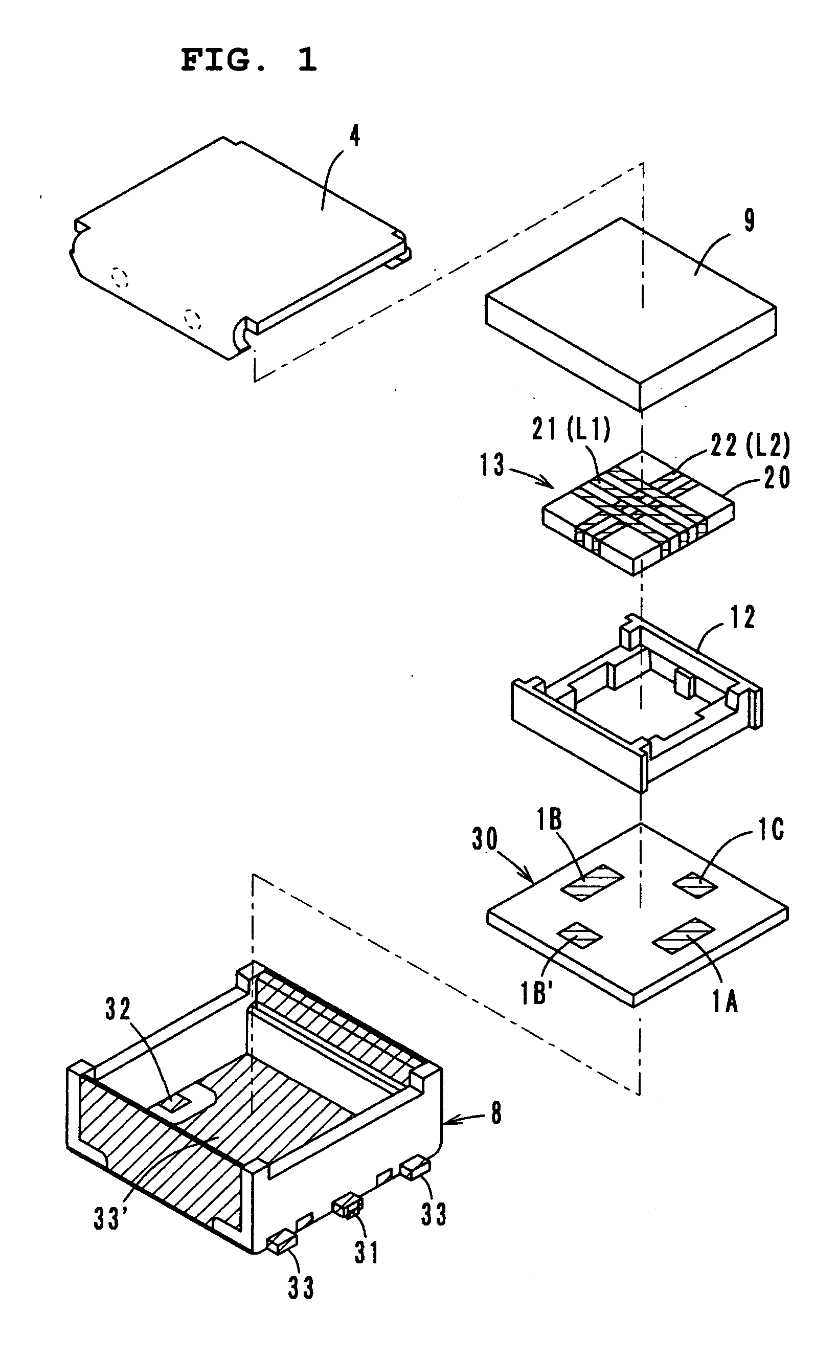
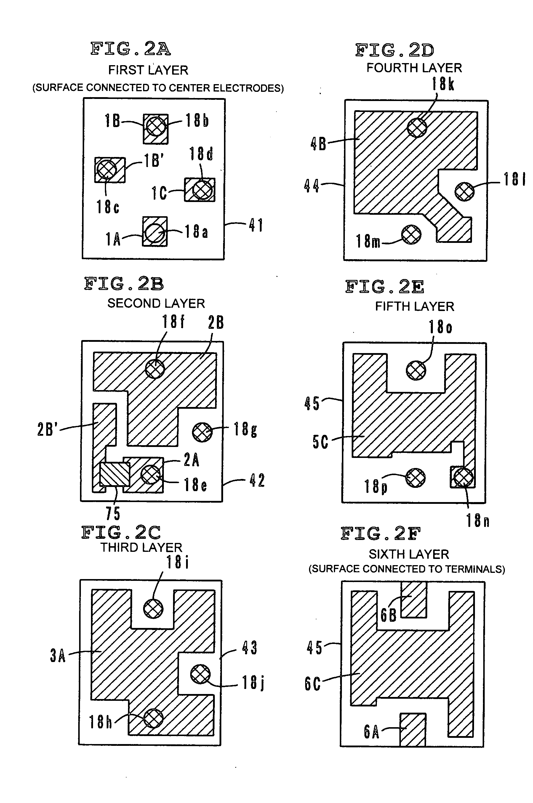
[0014] Specifically, a dielectric used for the second matching capacitor may have a higher Q factor than a dielectric that used for the first matching capacitor. In this case, it is more advantageous in a manufacturing process to form the first and second matching capacitors in a single laminated substrate. Each of the first and second matching capacitors may be formed into a single product as a single-plate capacitor or a laminated capacitor. The dielectric materials of these products may be the same or different, but the electrode configurations differ from each other, thus allowing the Q factor to be different from the first matching capacitor to the second matching capacitor.
[0017] In the two-port isolator according to preferred embodiments of the present invention, furthermore, a via hole connected with the electrodes that define the second matching capacitor are preferably larger than a via hole connected with the electrodes that define the first matching capacitor. The larger the via hole connected with an electrode, the higher the Q factor of the matching capacitor defined by this electrode, which leads to lower insertion loss. The first matching capacitor preferably has a relatively low Q factor, and the via hole connected with the electrodes for the first matching capacitor is preferably small. Thus, the area of the matching capacitor electrode in the dielectric layer with the via hole extending therethrough is increased. In other words, the required matching capacitors are obtained without increasing the number of sheets for the matching capacitor electrodes or increasing the size of the laminated substrate.
[0018] Another preferred embodiment of the present invention provides a communication device including the two-port isolator, which is also compact and low-cost.
[0019] According to various preferred embodiments of the present invention, therefore, the insertion loss is reduced during signal propagation from the input port to the output port. Moreover, the second matching capacitor preferably has a higher Q factor than the first matching capacitor, and the first matching capacitor is preferably made of an inexpensive material of low Q factor and / or relatively high dielectric constant. Thus, a compact and low-cost isolator in which the insertion loss is slow is realized.
Problems solved by technology
The isolator shown in FIG. 17 of this publication, which is well known in the art, has a problem in that two resonance circuits are resonated during signal propagation from an input port to an output port, which causes high power loss and high insertion loss.
However, due to the use of a high-purity starting material and a high-precision manufacturing process, high-Q dielectric material increases the production cost of the isolator.
This makes it difficult to reduce the size and cost of the isolator.
In a case where the matching capacitor electrodes are formed in a multilayer substrate, if the area of via holes connected with the matching capacitor electrodes is small, a large conductor loss occurs in the via holes, and high-Q matching capacitors are not obtained.
Thus, the required capacitance is not obtained.
The larger the via hole connected with an electrode, the higher the Q factor of the matching capacitor defined by this electrode, which leads to lower insertion loss.
However, it is undesirable that the dielectric sheet that define the second matching capacitor C2 be made of such a dielectric material.
It is therefore necessary to increase the number of dielectric sheets or increase the size of the multilayer substrate 30 in order to obtain the desired matching capacitance, thus making it difficult to obtain a size-reduced and low-cost isolator.
On the other hand, the area of the via holes connected to the electrodes for the second matching capacitor increases, thus increasing the Q factor of the second matching capacitor, which leads to low insertion loss.
If the capacitor electrode to be trimmed is formed in a deep layer, a high-power laser oscillator is required or the trimming time must be increased, thus increasing the cost.
Method used
View moreImage
Smart ImageViewing Examples

Examples
Embodiment Construction
[0079] The present invention is not limited to the two-port isolator according to the foregoing preferred embodiments, and it is to be understood that a variety of modifications may be made without departing from the spirit and scope of the invention.
Login to View More PUM
 Abstract
A two-port isolator includes a microwave ferrite member, first and second center electrodes that intersect with each other on the ferrite member with isolation therebetween, a permanent magnet that applies a DC magnetic field to the ferrite member, and a multilayer substrate having center-electrode-connecting electrodes and first and second matching capacitors. The ferrite member, the first and second center electrodes, the permanent magnet, and the multilayer substrate are accommodated in a housing that includes a magnetic cap and a case having a magnetic metal plate molded thereonto. The second matching capacitor has a higher Q factor than the first matching capacitor.
Description
[0001] 1. Field of the Invention[0002] The present invention generally relates to two-port isolators, and, more specifically, to a two-port isolator for use in the microwave band and to a communication device.[0003] 2. Description of the Related Art[0004] Generally, non-reciprocal circuit elements, such as isolators and circulators, have a characteristic that permits a signal to transmit only in a predetermined direction but not in the opposite direction. Such circuit elements are used in transmitting circuits of mobile communication devices, such as mobile telephones and cellular telephones. One type of non-reciprocal circuit element is the two-port circuit element disclosed in, for example, Japanese Unexamined Patent Application Publication No. 9-232818. Equivalent circuits of such a circuit element, namely, a two-port isolator, are shown in FIGS. 11 and 17 of this publication.[0005] The isolator shown in FIG. 17 of this publication, which is well known in the art, has a problem i...
Claims
Login to View More Application Information
Patent Timeline
 Patent Type & AuthorityApplications(United States)
IPC IPC(8): H01P1/36H01P1/365
CPCH01P1/36
InventorHINO, SEIGO
OwnerMURATA MFG CO LTD