Amplification-type solid-state image pickup device incorporating plurality of arrayed pixels with amplification function

Inactive Publication Date: 2005-01-06
SHARP KK
View PDF6 Cites 9 Cited by
  • Summary
  • Abstract
  • Description
  • Claims
  • Application Information

AI Technical Summary

Benefits of technology

In an amplification-type solid-state image pickup device in one embodiment, drains of the field effect transistors for amplification are each connected on a column basis to the drain lines.
In an amplification-type solid-state image pickup device in one embodiment, drains of the field effect transistors for reset are each connected on a row basis to reset drain lines extending in row direction, and there is provided a third scanning circuit for sequentially applying two pulsed driving voltages to the drains of the field effect transistors for reset on a row basis through the reset drain lines.
In the amplification-type solid-state image pickup device in this one embodiment, the drain potentials of the field effect transistors for reset are controlled on a row basis by the third sc

Problems solved by technology

However, if the potential of the reset drain 206 is fixed to VDD by the soft reset operation, leakage in the reset gate due to sub-threshold current disa

Method used


Image

  • Amplification-type solid-state image pickup device incorporating plurality of arrayed pixels with amplification function
  • Amplification-type solid-state image pickup device incorporating plurality of arrayed pixels with amplification function
  • Amplification-type solid-state image pickup device incorporating plurality of arrayed pixels with amplification function

Examples


first embodiment

(First Embodiment)

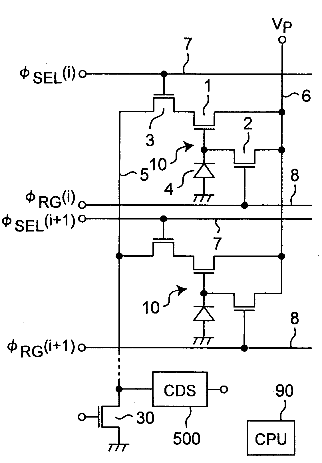
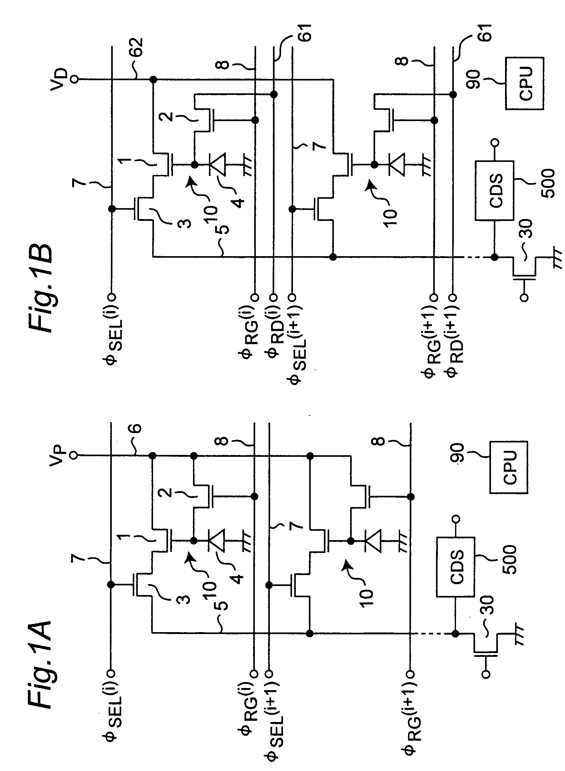
FIG. 1A shows the circuit constitution of an APS (Active Pixel Sensor)-type two-dimensional image sensor in one embodiment of the present invention. Although the image sensor incorporates a plurality of pixels disposed in matrix form, only two pixels 10 of two rows by one column are shown for easier understanding. Row direction corresponds to horizontal direction while column direction corresponds to vertical direction.

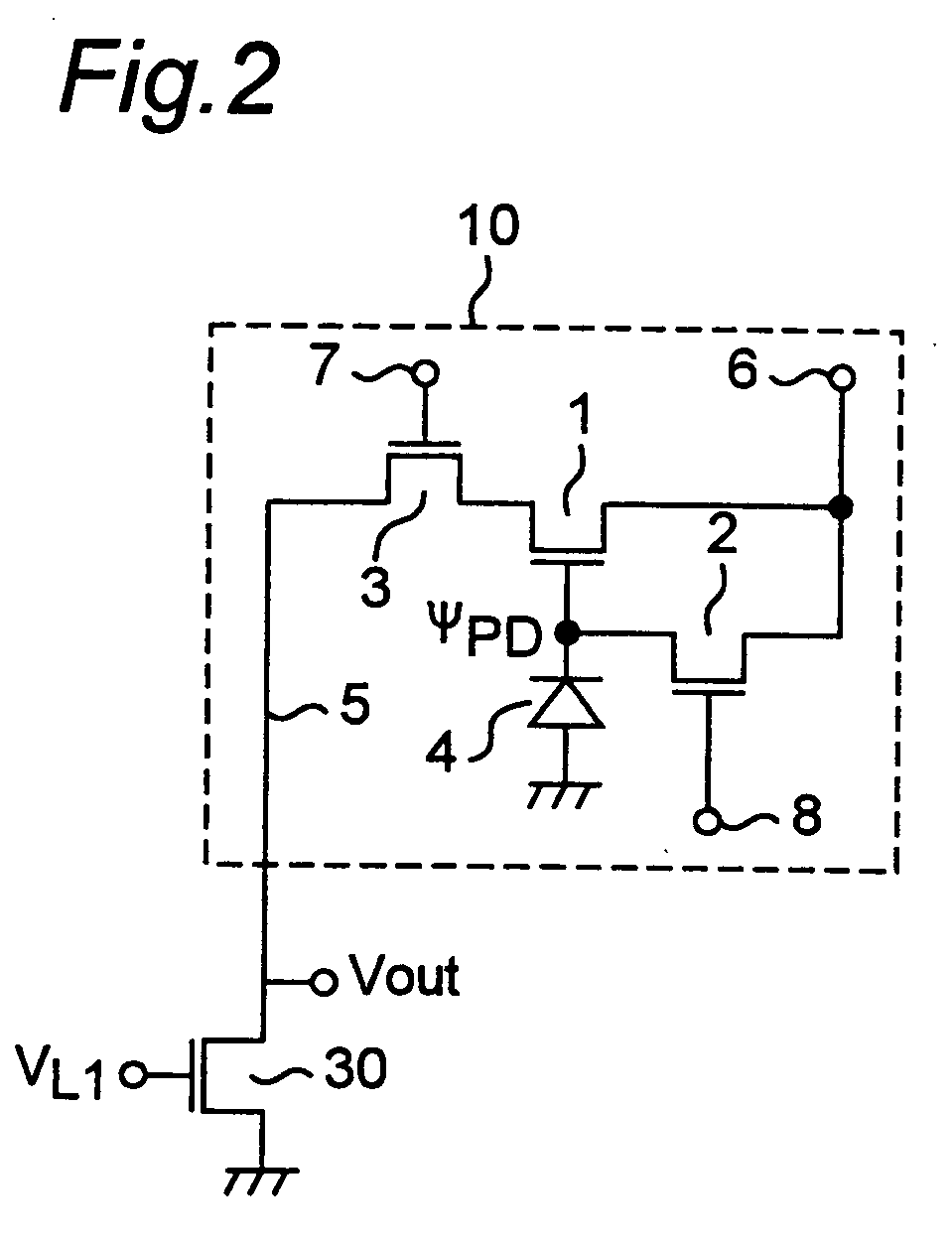
As shown in FIG. 2, each pixel 10 is composed of one photodiode (PD) 4 serving as a photon-electron conversion region, and three N channel-type MOS transistors (Tr) 1, 2, 3 (PD+3Tr type), more specifically, a MOS transistor for signal amplification 1, a MOS transistor for reset 2, and a MOS transistor for pixel selection 3.

The anode of the photodiode 4 is grounded and the cathode is connected to the MOS transistor for signal amplification 1. The MOS transistor for signal amplification 1 amplifies a signal representing a potential of the photodiod...

second embodiment

(Second Embodiment)

In the aforementioned method in which the soft reset operation and hard reset operation are combined, image retention and reset noise are avoidable. However, there is the possibility that linearity of output signals with respect to incident optical signals might be damaged.

As shown in FIG. 5A and FIG. 5B in details, due to a sub-threshold current during the third reset period TR3, the photodiode potential ψPD (A) immediately after the period TR3 in the preceding frame F(n) becomes lower by ΔV1 (see FIG. 6) than the channel potential ψRG (H) obtained by the reset gate potential RG (H). The photodiode potential immediately before the first reset period TR1 in the noticed frame F(n+1) drops due to the charges generated by an incident optical signal during optical signal storage period TCHG after the third reset period TR3 in the preceding frame F(n). If the potential drop amount is not less than ΔV1, then the photodiode potential immediately after the first reset ...


PUM


Abstract

An amplification-type solid-state image pickup device of the present invention repeats, in every frame, a signal level readout period, a first reset period, a reset level readout period, a second reset period, and a third reset period in this order. In the first reset period and the third reset period, a MOS transistor for reset is set to execute a soft reset operation with a sub-threshold current, while in the second reset period, the MOS transistor for reset is set to execute a hard reset operation so as to fix the potential of a photon-electron conversion region to a drain potential. This makes it possible to reduce both reset noise and image retention with a simple constitution.

Description

This Nonprovisional application claims priority under 35 U.S.C. §119(a) on Patent Application No. 2003-190171 filed in Japan on Jul. 2nd 2003 and Patent Application No. 2003-357652 filed in Japan on October 17th, the entire contents of which are hereby incorporated by reference. BACKGROUND OF THE INVENTION The present invention relates to an amplification-type solid-state image pickup device, and more specifically relates to an amplification-type solid-state image pickup device incorporating a plurality of arrayed pixels with an amplification function. There has been proposed an amplification-type solid-state image pickup device having a pixel portion in which each pixel has an amplification function and a scanning circuit disposed around the pixel portion, the pixel portion being scanned by the scanning circuit so that each pixel data is read out. Particularly, there is known an APS (Active Pixel Sensor)-type image sensor having a pixel constitution composed of a CMOS that offer...

Claims


Application Information

Patent Timeline
IPC IPC(8): H01L27/00H01L27/146H04N5/363H04N5/374H04N5/378
CPCH01L27/14601H04N5/374H04N5/363H04N5/3597H04N25/626H04N25/65H04N25/76H01L27/146H04N25/75
Inventor WATANABE, TAKASHI
Owner SHARP KK
Why Eureka
Try Eureka