Inspection method and apparatus of laser crystallized silicons

a laser crystallization and inspection method technology, applied in the direction of individual semiconductor device testing, semiconductor/solid-state device testing/measurement, instruments, etc., can solve the problem of poor crystallization quality, and achieve the effect of simple and prompt method

Active Publication Date: 2005-01-06
AU OPTRONICS CORP
View PDF2 Cites 31 Cited by
  • Summary
  • Abstract
  • Description
  • Claims
  • Application Information

AI Technical Summary

Benefits of technology

[0006] It is an object of the present invention to provide an inspection method of laser crystallized silicons applied in the low-temperature poly Si (LTPS) process. By the phenomenon of similar beam splitting-gratings caused by the protrusion arrangement at the surface of the crystallized silicons formed on an insulating substrate through the line scanning of the excimer laser annealing (ELA) technology, a simple and prompt method for examining the crystalline quality of the surface of the crystallized silicons is provided.

Problems solved by technology

For instance, when the variations of the reflected light are large and obvious, stripes are distributed over the surface of the crystallized silicons and this represents a poor quality of crystallization.

Method used


Image

  • Inspection method and apparatus of laser crystallized silicons
  • Inspection method and apparatus of laser crystallized silicons
  • Inspection method and apparatus of laser crystallized silicons

Examples


Embodiment Construction

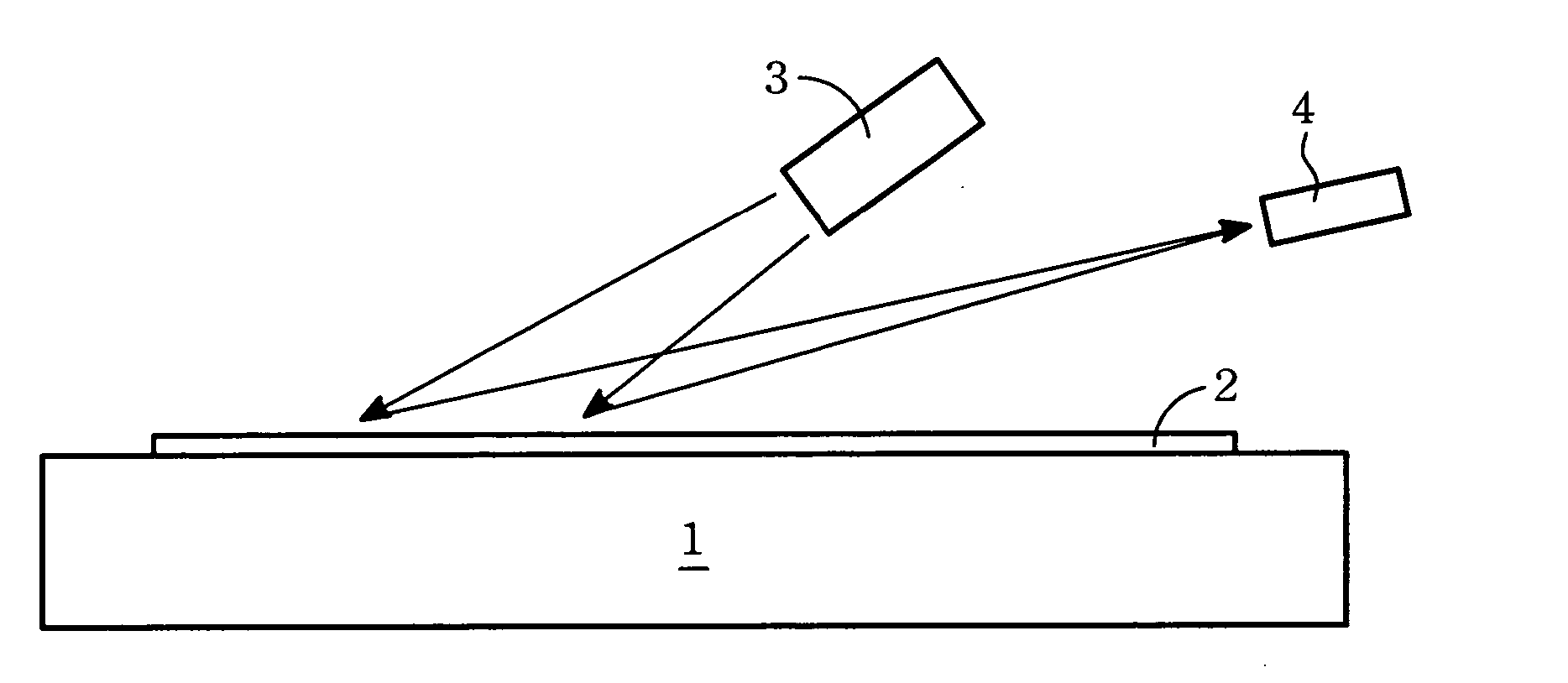
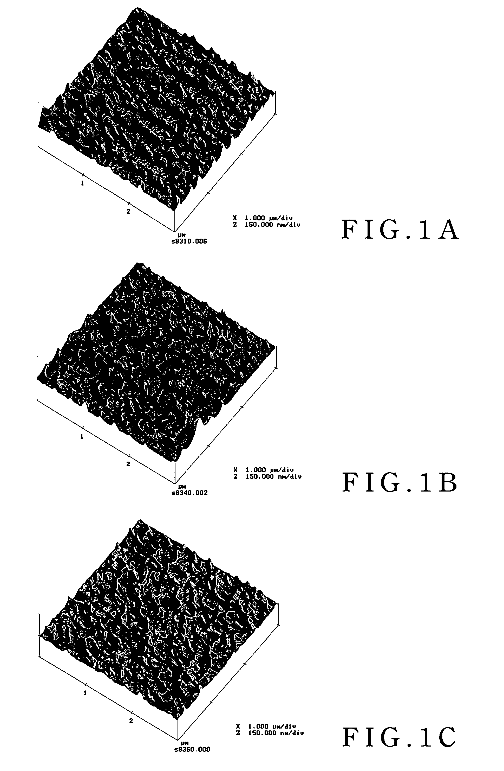
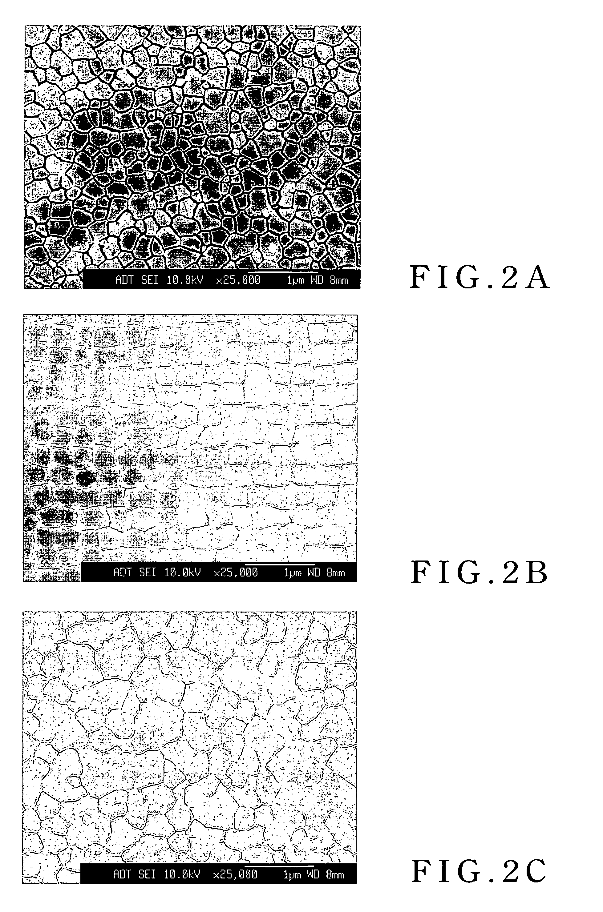
[0017] A novel inspection method of laser crystallized silicons is provided in this invention. In the process for irradiating the amorphous silicons on an insulating substrate such as glass substrate with a laser beam through an excimer laser annealing (ELA) technology of line scanning to be crystallized, a visible light source such as a white light is used to irradiate the surface of the crystallized silicons, and the quality of the crystallization is examined by variations of the light reflected by the protrusion arrangement at the surface of the crystallized silicons. For instance, when the intensity of the reflected light is large and obvious, stripes are distributed over the surface of the crystallized silicons and this represents a poor quality of crystallization. Moreover, whether the laser energy of the laser beam used in the ELA technology does not match the crystallization conditions of the amorphous silicons or the laser energy thereof is unstable can also be monitored.

[...


PUM

PropertyMeasurementUnit
angleaaaaaaaaaa
angleaaaaaaaaaa
optical path differenceaaaaaaaaaa

Abstract

An inspection method and apparatus of laser crystallized silicons in the low-temperature poly Si (LTPS) process. The crystalline quality is inspected by using a visible light source to irradiate the surface of the poly Si and examining the variations of the reflected light caused by the protrusion arrangement at the surface of the poly Si. This method can be adopted on the poly Si samples prepared by the line scanning of the excimer laser annealing (ELA) technology.

Description

FIELD OF THE INVENTION [0001] The present invention relates to an inspection method and apparatus of laser crystallized silicons and, more specifically, to an inspection method for synchronously monitoring the formation of laser crystallized silicons in the low-temperature poly Si (LTPS) process and an inspection apparatus using thereof. BACKGROUND OF THE INVENTION [0002] With the advance of techniques for manufacturing thin-film transistors, the liquid crystal displays (LCD) are widely applied in various electronic products, such as calculators, personal digital assistants (PDAs), watches, laptops, digital cameras, and mobile phones, etc. due to their advantages as smaller size, less weight, lower power consumption and no radiation. Furthermore, since manufacturers aggressively invest in research & development and employ large-scale fabricating equipment, the decreasing cost of production makes the TFT-LCD devices more popular. [0003] Since the low-temperature poly Si (LTPS) thin f...

Claims


Application Information

Patent Timeline
Patent Type & Authority Applications(United States)
IPC IPC(8): G02F1/13G01N21/95H01L21/20H01L21/268
CPCG01N21/95H01L21/268H01L21/2026H01L21/02686H01L21/02691H01L21/02422H01L21/02532G02F1/13
Inventor TSAO, I-CHANG
Owner AU OPTRONICS CORP
Why Eureka
Try Eureka