Method of tuning optical components integrated on a monolithic chip

a monolithic chip and optical component technology, applied in semiconductor lasers, electromagnetic repeaters, instruments, etc., can solve the problems of difficult to manufacture arrays of dfb laser sources with wavelength grids, and dfb laser arrays with wavelength grids. , to achieve the integration of a dfb laser array with an awg optical multiplexer with their respective wavelength grids, the problem of repeated manufacturing

Inactive Publication Date: 2005-01-20
INFINERA CORP
View PDF8 Cites 27 Cited by
  • Summary
  • Abstract
  • Description
  • Claims
  • Application Information

AI Technical Summary

Benefits of technology

[0079] According to this invention, a monolithic transmitter photonic integrated circuit (TxPIC) chip comprises an array of modulated sources formed on the PIC chip and having different operating wavelengths according to a standardized wavelength grid and providing signal outputs of different wavelengths. Pluralities of wavelength tuning elements are integrated on the chip, one associated with each of the modulated sources. An optical combiner is formed on the PIC chip and the signa

Problems solved by technology

The principal reason is that it is difficult to fabricate, on a repeated basis, an array of DFB lasers with a wavelength grid that simultaneously matches the wavelength grid of the a wavelength selective combiner (e.g., an AWG).
However, these types of laser sources are more difficult to manufacture in an array and in monolithic form compared to DFB laser sources.
But again, the integration of a DFB

Method used


Image

  • Method of tuning optical components integrated on a monolithic chip
  • Method of tuning optical components integrated on a monolithic chip
  • Method of tuning optical components integrated on a monolithic chip

Examples


Embodiment Construction

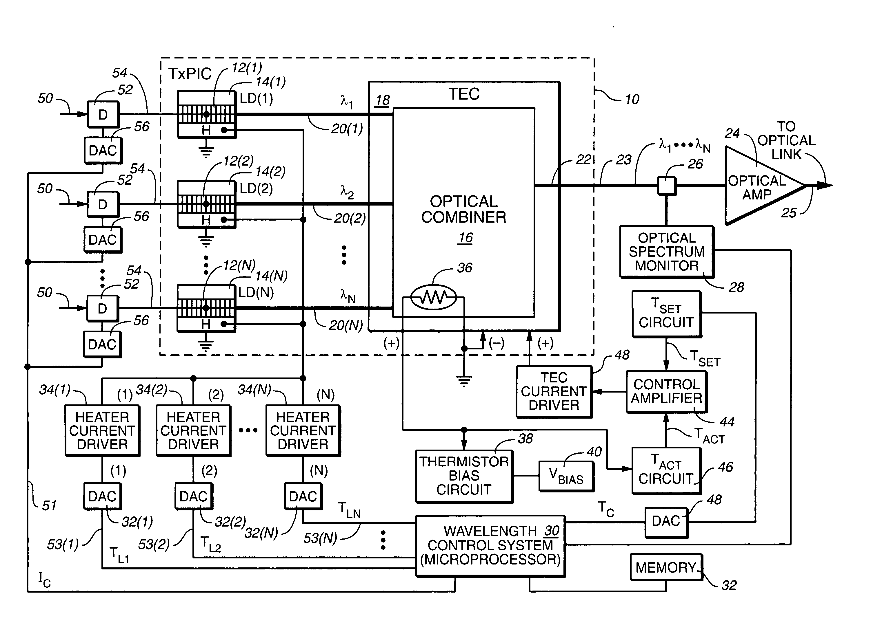
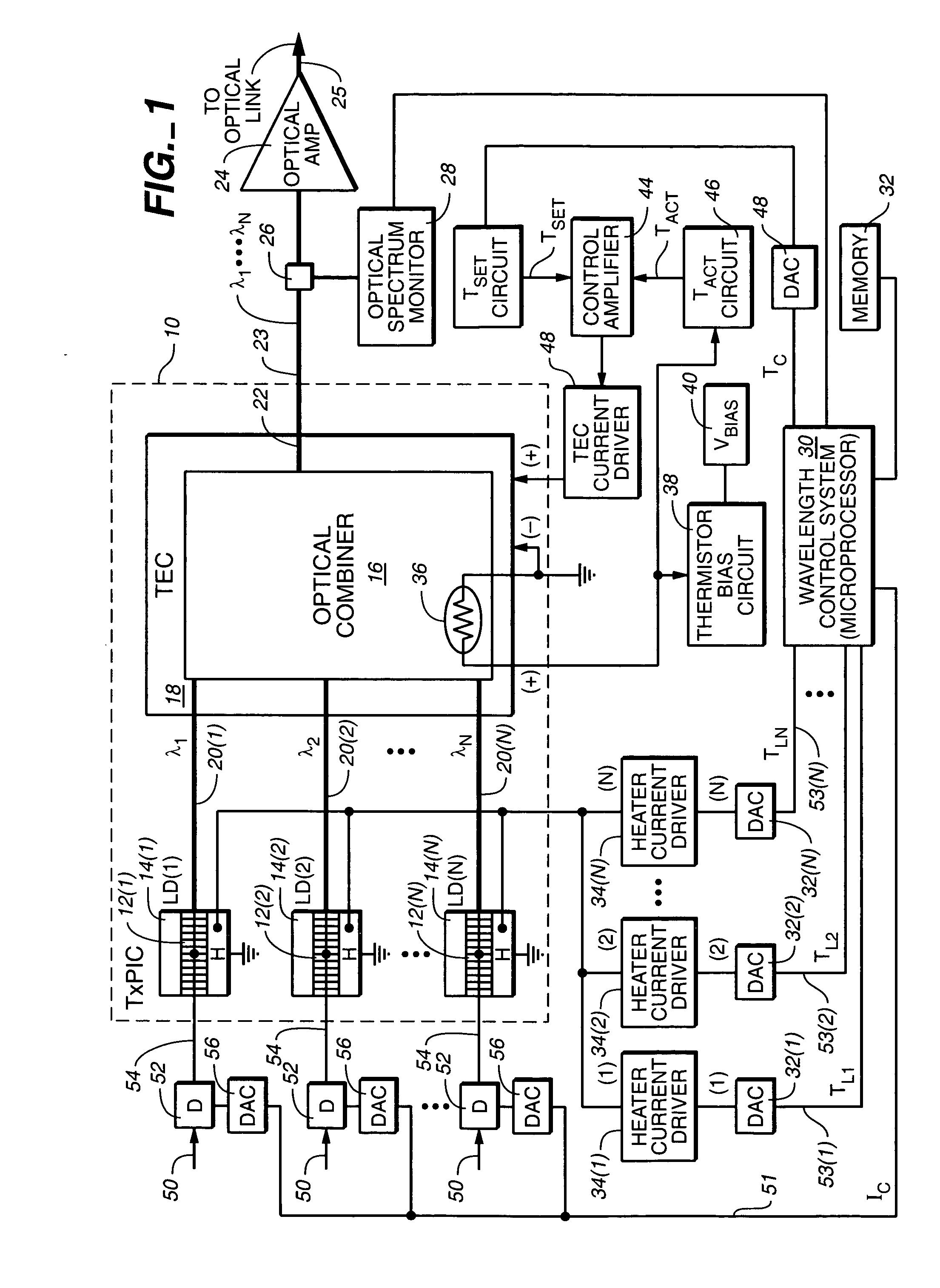
[0115] Reference is now made to FIG. I wherein there is shown an example of an embodiment of this invention comprising TxPIC chip 10 utilizing wavelength tuning elements for tuning the modulated source grid with the multiplexer grid, which are shown in FIG. 1 as thermal tuning elements. However, it should be understood that other wavelength tuning elements are contemplated in this invention, such as modulated source tuning by means of changing laser current and bias to change its refractive index and, therefore, the operating wavelength of a laser. Other wavelength tuning elements include: adding multiple sections to the laser and varying the current in each section (including, phase tuning, which is the provision of a phase section in a DFB or DBR laser), vernier tuning where the best passband response is chosen from multiple outputs of the optical multiplexer, the use of coolers to tune the wavelength grid or individual elements of the PIC, including TECs which are also shown in c...


PUM


Abstract

A method of tuning optical components integrated on a monolithic chip, such as an optical transmitter photonic integrated circuit (TxPIC), is disclosed where a group of first optical components are each fabricated to have an operating wavelength approximating a wavelength on a standardized or predetermined wavelength grid and are each included with a local wavelength tuning component also integrated in the chip. Each of the first optical components is wavelength tuned through their local wavelength tuning component to achieve a closer wavelength response that approximates their wavelength on the wavelength grid.

Description

REFERENCE TO RELATED APPLICATION [0001] This application is a division of U.S. parent patent application, Ser. No. 10 / 267,330, filed Oct. 8, 2002, which application claims priority to provisional application Ser. No. 60 / 328,207, filed Oct. 9, 2001, now U.S. patent application, Ser. No. 10 / 267,331, filed Oct. 8, 2002 and entitled, TRANSMITTER PHOTONIC INTEGRATED CIRCUIT (TxPIC) CHIP ARCHITECTURES AND DRIVE SYSTEMS AND WAVELENGTH STABILIZATION FOR TxPICs; provisional application, Ser. No. 60 / 328,332, filed Oct. 9, 2001, now part of U.S. patent application, Ser. No. 10 / 267,331, supra; provisional application, Ser. No. 60 / 370,345, filed Apr. 5, 2002, the provisional application corresponding to U.S. patent application, Ser. No. 10 / 267,330; provisional application, Ser. No. 60 / 378,010, filed May 10, 2002, now U.S. patent application, Ser. No. 10 / 267,346, filed Oct. 8, 2002 and entitled, TRANSMITTER PHOTONIC INTEGRATED CIRCUIT (TxPIC) CHIP WITH ENHANCED POWER AND YIELD WITHOUT ON-CHIP AMP...

Claims


Application Information

Patent Timeline
IPC IPC(8): G02B6/12G02B6/34G02F1/017H01S3/10H01S3/13H01S5/00H01S5/024H01S5/026H01S5/06H01S5/0625H01S5/0683H01S5/12H01S5/20H01S5/22H01S5/227H01S5/34H01S5/40H01S5/50H04B10/04H04B10/12H04B10/145H04B10/17H04B10/29H04J14/02
CPCB82Y20/00H04J14/02G02B6/12004G02B6/12007G02B6/12019G02B6/12023G02B6/12026G02B6/12028G02B6/12033G02B6/124G02F1/01725G02F2001/0175G02F2001/01758H01S5/0085H01S5/024H01S5/02415H01S5/02453H01S5/02461H01S5/02476H01S5/026H01S5/0261H01S5/0264H01S5/0265H01S5/0268H01S5/0425H01S5/0612H01S5/06256H01S5/06258H01S5/0683H01S5/0687H01S5/12H01S5/1228H01S5/2077H01S5/22H01S5/2214H01S5/2224H01S5/227H01S5/2272H01S5/2275H01S5/3408H01S5/34306H01S5/4025H01S5/4031H01S5/4087H01S5/50H04B10/2914H04B10/50H04B10/506H04B10/572G02B6/02204H01S5/04256G02F1/0175G02F1/01758
Inventor KISH, FRED A. JR.JOYNER, CHARLES H.WELCH, DAVID F.WEBJORN, JONASTAYLOR, ROBERT B.NILSSON, ALAN C.
Owner INFINERA CORP
Why Eureka
Try Eureka